In our increasingly interconnected world, Printed Circuit Boards (PCBs) are the invisible backbone of almost every electronic device. From the smartphones we rely on to the intricate machinery that powers industries, PCBs are crucial. Understanding both PCB manufacturing and assembly is key for anyone involved in electronics development and production. This article serves as a comprehensive guide, detailing the nuances of each step, offering clarity, and helping you navigate the world of PCB creation effectively.
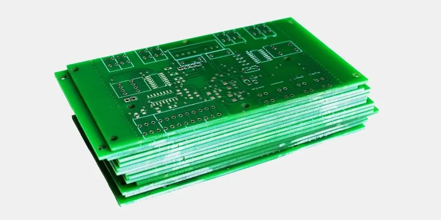
PCB manufacturing is the foundational process of creating the bare printed circuit board, transforming design specifications into a physical substrate ready for component assembly. This intricate process involves multiple stages, from selecting appropriate base materials to the final testing of the bare board, and requires precision and adherence to strict quality standards to ensure the functionality and reliability of the final electronic product. The process is distinct from PCB assembly, which involves adding electronic components to the manufactured board.
| Process Stage | Description |
|---|---|
| Substrate Selection | Choosing the base material, typically a composite like FR-4, based on thermal, mechanical, and electrical requirements. |
| Image Transfer | Transferring the circuit design onto the substrate using methods like photolithography, where a photosensitive material is exposed to UV light through a photomask. |
| Etching | Removing unwanted copper from the board using chemical etching processes, leaving only the desired circuit traces. |
| Layer Lamination | Pressing together multiple layers of PCBs in a multilayer board using heat and pressure to achieve the necessary copper trace connections and isolation. |
| Drilling | Creating holes in the PCB for component placement and electrical connections, employing precision drilling tools. |
| Plating | Applying a conductive coating to the drilled holes and surface to facilitate electrical connections |
| Solder Mask Application | Applying a solder mask, a protective layer that prevents solder bridges between traces, enhancing assembly process. |
| Silkscreen Printing | Printing component designators and logos on the board using silkscreen ink for easy identification during assembly and debugging. |
| Final Testing | Verifying the board's integrity and electrical connections through testing, including short and open circuit tests. |
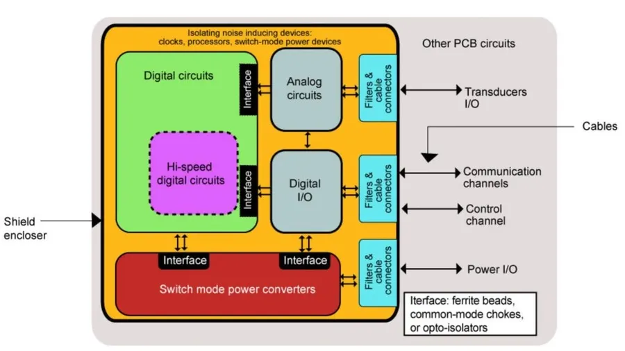
The PCB assembly process is the critical stage where electronic components are mounted onto a bare printed circuit board (PCB), transforming it into a functional electronic module. This process involves several intricate steps, from component placement to soldering and quality inspection, ensuring the final product meets design specifications and performance requirements. Key techniques include Surface Mount Technology (SMT), through-hole assembly, and manual assembly for specialized needs.
| Assembly Technique | Description | Typical Application |
|---|---|---|
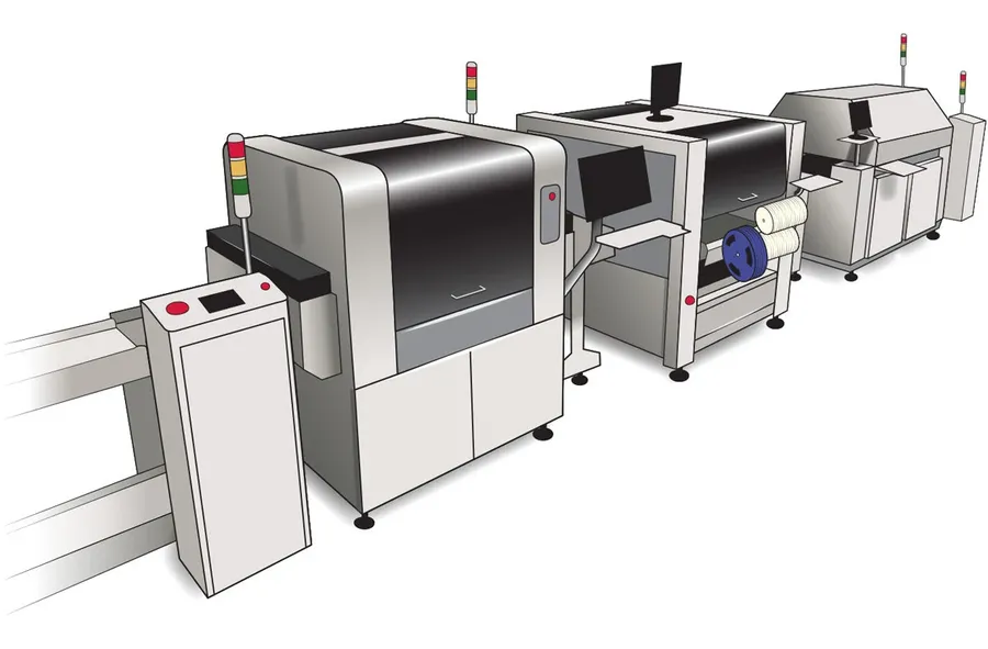
| Surface Mount Technology (SMT) | Components are mounted directly onto the surface of the PCB. | High volume manufacturing of consumer electronics. |
| Through-hole Technology | Components are inserted through drilled holes and soldered on the opposite side. | Applications requiring robust mechanical connections. |
| Hand Assembly | Components are manually placed and soldered onto the PCB. | Prototyping, low-volume orders, specialized components. |
| Wave Soldering | PCB passed over a wave of molten solder | Through-hole component soldering in high volume. |
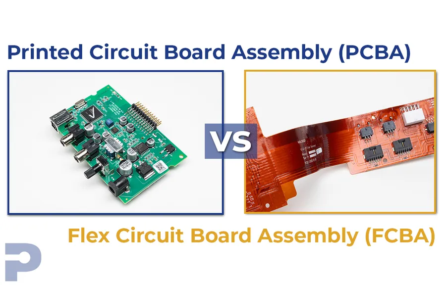
The core distinction between PCB manufacturing and PCB assembly lies in their respective focuses: manufacturing creates the bare circuit board, while assembly populates that board with electronic components. These two processes are sequentially dependent; the board must be manufactured before it can be assembled.
| Aspect | PCB Manufacturing | PCB Assembly |
|---|---|---|
| Primary Goal | Creation of the bare PCB | Population of the PCB with components |
| Input | PCB design files (e.g., Gerber files) | Bare PCB, Bill of Materials (BOM), component placement data |
| Key Processes | Substrate selection, Image transfer, Etching, Drilling, Plating, Solder mask application | Component sourcing, Solder paste application, Component placement (SMT & Through-hole), Reflow soldering, Wave soldering, AOI, Functional testing |
| Output | Bare printed circuit board | Fully populated PCB assembly |
| Interdependence | Independent Process with dependent on PCB design | Dependent on PCB manufacturing |
The cost of PCB manufacturing and assembly is influenced by a multitude of factors, each playing a significant role in the final price. Understanding these factors is crucial for cost optimization and effective budgeting. This section breaks down these variables, offering insight into how each one affects the overall expenditure.
| Cost Factor | Description | Impact on Cost |
|---|---|---|
| Material Selection | The type of substrate (e.g., FR-4, aluminum), copper thickness, and other materials used. | High-performance materials or unique substrates significantly increase cost. |
| Design Complexity | The number of layers, board dimensions, via density, trace width and spacing, and component footprint complexity. | More complex designs (e.g., high layer count) lead to increased manufacturing time and cost. |
| Quantity of Boards | The volume of PCBs produced in one order. | Larger quantities usually lead to lower per-unit cost due to economies of scale. |
| Lead Times | The time required for manufacturing and assembly. | Expedited lead times (rush orders) typically incur higher costs. |
| Component Sourcing | The cost of electronic components and how they are sourced. | Components with long lead times, rare, or from unofficial sources, increase total cost. |
| Assembly Method | Surface Mount Technology (SMT) vs. Through-Hole Technology (THT), manual vs. automated | Automated assembly with SMT is generally more cost-effective for higher volumes. |
| Testing Requirements | The depth and type of tests required (e.g., electrical tests, AOI, functional tests). | More rigorous testing can add to the overall cost. |
| Surface Finish | The type of surface plating (e.g., HASL, ENIG, Immersion Silver). | Finishes like ENIG are more expensive than HASL. |
To optimize costs, consider these tips: 1. Design for manufacturability (DFM): Simplify your PCB design by adhering to standard trace widths, clearances, and component footprints, reducing production complexities. 2. Optimize board size: Minimize the board dimensions to save on material and production expenses. 3. Standardize component selection: Select readily available and reasonably priced electronic components. 4. Plan for volume: If future demand allows, increase the batch quantity to benefit from economies of scale. 5. Plan your lead times realistically: Avoid rush orders by planning well in advance. 6. Evaluate surface finishes: Choose surface finishes appropriate for your project requirements, potentially avoiding more costly options where they are not necessary.
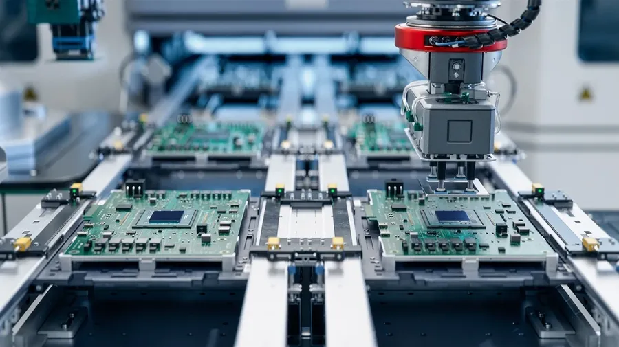
Selecting the ideal PCB manufacturing and assembly service is critical for project success, directly impacting quality, cost, and timelines. This section provides a framework for evaluating providers, emphasizing expertise, technology, certification, lead times, and support.
When selecting a PCB manufacturing and assembly service provider, consider the following criteria, ensuring they align with your project's requirements and constraints:
By carefully considering these criteria, you can select a PCB manufacturing and assembly partner that best aligns with your specific project needs, reducing the risk of delays and quality issues while ensuring cost-effectiveness.
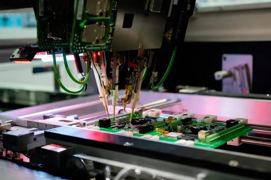
Rigorous quality control and testing are paramount in both PCB manufacturing and assembly to ensure the reliability and functionality of the final product. These measures span from the bare board production to the fully assembled PCB, encompassing electrical, visual, and functional assessments.
The purpose of quality control is to identify defects early in the process, which reduces the cost and effort to fix these issues later on, and ensures the PCBs meet required standards.
| Test Type | Description | Purpose | Stage |
|---|---|---|---|
| Electrical Tests | Continuity tests to verify the connections, Impedance testing and shorts detection. | Ensures signal integrity and proper function, prevents short circuits. | Bare board & assembled board |
| X-Ray Inspection | Non-destructive testing, using x-rays, to check the interior of the PCB for defects. | Identifies hidden defects such as solder voids, misaligned components, and shorts in BGAs or other complex packages. | Assembled board |
| Automated Optical Inspection (AOI) | Automated visual inspection to check for component placement, soldering quality, and other visible defects. | Ensures accuracy and reduces manual inspection time. | Assembled board |
| Functional Testing | Verifies the functional performance of the assembled PCB, often using test jigs and fixtures, simulating real operational conditions. | Confirm the operation of the board according to it's intended purpose and find out any failure modes before releasing to clients. | Assembled board |
| Visual Inspection | A basic but crucial test where boards are checked visually for any defects such as scratches or misalignments. | Identifies physical defects that could affect performance | Bare board & assembled board |
This section addresses common inquiries regarding PCB manufacturing and assembly, providing clear and concise answers to help clarify the processes involved.
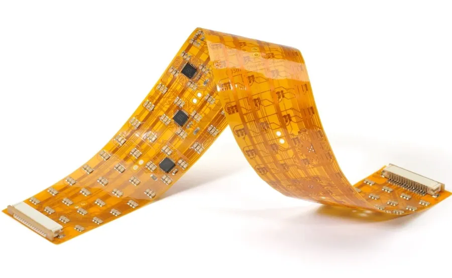
The PCB manufacturing and assembly landscape is continually evolving, driven by demands for increased functionality, miniaturization, and sustainability. These trends and innovations are shaping the future of electronics, demanding that manufacturers adapt to remain competitive. Understanding these advancements is crucial for businesses and engineers alike, enabling them to anticipate future requirements and optimize their processes.
Understanding PCB manufacturing and assembly is critical for creating high-quality, functional electronic products. Whether you need a quick PCB prototype or a large-scale production run, mastering these two processes helps ensure cost-effectiveness and reliability. As technology continues to advance, the processes involved in both PCB manufacturing and assembly will continue to evolve, making it essential to stay informed and adaptable. By embracing new techniques and maintaining a focus on quality, you can leverage the full potential of PCB technology in various applications.

