In the fast-paced world of electronics, a rapid PCB prototype is crucial for bringing your designs to life. From hobbyists to seasoned engineers, the ability to quickly test and iterate is paramount. This article delves into the world of PCB prototyping, exploring available options, costs, and best practices for obtaining your first circuit board. We bridge the gap between your ideas and tangible products, with cost-effective solutions and rapid turnarounds for that all-important [pcb prototype].
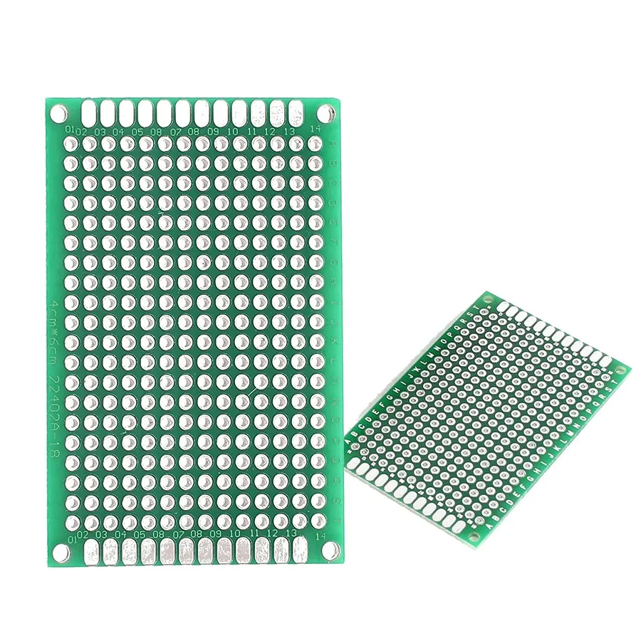
A Printed Circuit Board (PCB) prototype is a preliminary version of a PCB, meticulously crafted to validate a circuit design before committing to mass production. It serves as a crucial step in the electronic design process, enabling engineers to identify design flaws, verify functionality, and optimize performance, ultimately mitigating risks and reducing costly errors during full-scale manufacturing.
The significance of PCB prototypes lies in their ability to bridge the gap between theoretical design and practical application. By creating a tangible representation of the circuit, engineers can conduct comprehensive testing under real-world conditions. This process provides valuable insights into the design's performance, ensuring it meets the intended specifications and functions as expected. Additionally, a successful PCB prototype can dramatically decrease the overall costs associated with production by allowing for early design corrections, preventing the manufacturing of defective or inefficient PCBs.
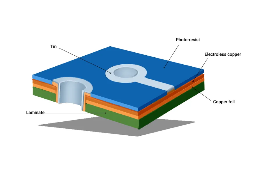
Selecting the appropriate PCB prototype service is crucial for the success of any electronics project. This choice significantly impacts both the development timeline and overall project cost. Careful evaluation of several key factors is essential to align service capabilities with specific project requirements, guaranteeing that the final prototype effectively validates the intended design.
| Factor | Description | Importance |
|---|---|---|
| Price | Cost per board, setup fees, and tooling costs. | Directly affects project budget; consider both unit price and total cost. |
| Turnaround Time | Time from order placement to delivery of boards. | Critical for project timelines; faster turnaround accelerates design iterations. |
| Minimum Order Quantity (MOQ) | Minimum number of boards required per order. | Important for low-volume projects; high MOQ can lead to unnecessary costs. |
| Material Quality | Type and quality of materials used in board fabrication. | Impacts performance and reliability; ensure materials meet design requirements. |
| Supported Design Software | Compatibility with design tools used (e.g., Eagle, Altium, KiCad). | Ensures seamless file transfer and reduces potential compatibility issues. |
| Layer Count Capabilities | Maximum number of layers the manufacturer can produce. | Must meet project requirements; affects design complexity. |
| Surface Finish Options | Available plating finishes (e.g., ENIG, HASL, Immersion Silver). | Impacts board durability, solderability and lifespan; align with application. |
| Component Sourcing | Ability to source and assemble components onto the board. | Streamlines assembly process; reduces effort to procure and mount components. |
| Testing & Verification | Testing services available to verify the functionality of prototype boards. | Helps identify any design flaws prior to production, crucial for project success. |
| Customer Support | Availability and responsiveness of customer service. | Essential for troubleshooting and addressing any order-related issues. |
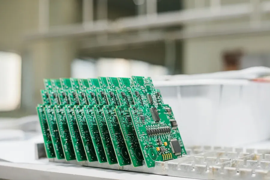
Quick-turn PCB prototyping is a streamlined manufacturing process designed to rapidly produce printed circuit board prototypes, significantly reducing the time between design completion and physical board availability. This accelerated turnaround is crucial for iterative design processes, allowing engineers to test and refine their circuits swiftly, thereby minimizing delays and accelerating product development cycles.
The primary benefit of quick-turn prototyping lies in its ability to compress the design-to-testing phase. By offering rapid fabrication, manufacturers enable engineers to promptly identify and rectify design flaws, evaluate component performance, and validate overall system functionality. This iterative approach minimizes the risk of costly late-stage design errors and ensures a higher probability of a successful final product.
Several PCB manufacturers specialize in quick-turn services. These companies differentiate themselves based on turnaround times, pricing models, and available features, catering to diverse prototyping needs.
| Company | Typical Turnaround Time | Cost Structure | Key Features |
|---|---|---|---|
| JLCPCB | 24-48 hours for standard PCBs | Highly competitive pricing, discounts for larger quantities | Wide range of material options, online ordering platform, PCB assembly options available. |
| PCBWay | 24-72 hours for standard PCBs | Competitive pricing, various shipping options. | Advanced PCB options (HDI, flex), online quoting, dedicated customer support. |
| OSH Park | ~1 week | Affordable, panelized service | Purple boards, excellent for hobbyists, smaller order quantities. |
To optimize the quick-turn PCB process, meticulous file preparation is essential. Here are a few key considerations:
Choosing the right quick-turn service requires careful evaluation of your project’s specific needs. By considering factors such as turnaround time, budget, and required features, you can expedite your design process while maintaining the necessary level of quality and precision.
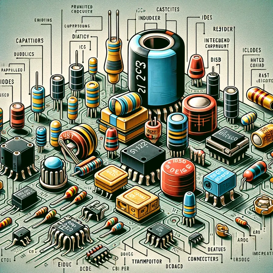
Achieving cost-effective PCB prototyping without sacrificing quality requires a strategic approach, focusing on design choices, material selection, and the judicious selection of prototyping services. The primary goal is to minimize expenses while ensuring the prototype accurately reflects the intended design functionality and performance.
Several strategies can be employed to reduce the cost of PCB prototyping. These include optimizing the design for manufacturability (DFM), selecting appropriate materials, and choosing prototyping services that offer competitive pricing without compromising quality. Careful consideration of these factors can significantly impact the overall prototyping budget.
| Cost Reduction Strategy | Description | Impact on Budget | Impact on Quality |
|---|---|---|---|
| Design Simplification | Reducing layer count, minimizing vias, using larger trace widths and clearances. | Significant cost reduction. | Minimal impact if design is not compromised. |
| Material Selection | Choosing standard materials (e.g., FR-4) over specialized options (e.g., high-Tg FR-4, Rogers) when performance requirements allow. | Moderate cost reduction. | Can affect high-frequency performance, thermal conductivity |
| Panelization | Designing multiple PCBs within a single panel to reduce per-unit cost. | Cost reduction proportional to panel size. | None, if handled correctly. |
| Component Selection | Selecting commonly available and cost-effective components. | Moderate to significant cost reduction. | Minimal to moderate impact depending on component performance |
| Batching Orders | Combining multiple prototype orders to take advantage of volume discounts. | Cost reduction on a per-order basis. | None. |
Several PCB prototyping services offer competitive pricing. For example, JLCPCB and PCBWay are known for their affordability, particularly for low-volume prototypes. However, it's essential to evaluate their offerings based on turnaround time, material options, and capabilities. Some cost-effective options might have longer lead times or limited material choices, which must be considered in relation to project deadlines and specifications.
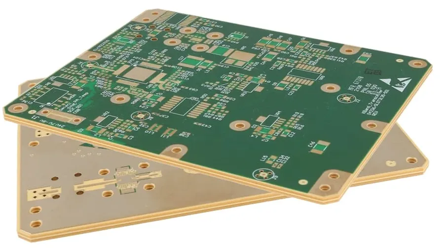
The selection of materials for a PCB prototype is a critical step that significantly influences the final product's performance, cost, and application suitability. Understanding the properties of common materials allows engineers to make informed decisions that align with design requirements and budgetary constraints.
| Material | Properties | Performance | Cost | Typical Applications |
|---|---|---|---|---|
| FR-4 | Rigid, flame-retardant, fiberglass-reinforced epoxy laminate | Good electrical insulation, moderate thermal resistance, versatile, widely used. | Low to moderate | General-purpose PCBs, most common applications. |
| Aluminum | Metal core, provides excellent heat dissipation | High thermal conductivity, good mechanical strength | Moderate to High | LED lighting, power electronics, applications with high heat generation. |
| Flexible Substrates (e.g., Polyimide) | Flexible and bendable, heat resistant | Excellent flexibility, good chemical resistance, suitable for dynamic applications | High | Wearable electronics, flexible circuits, applications requiring bending and folding. |
| Rogers Materials | High-frequency laminates with low dielectric constant and loss | Superior electrical performance at high frequencies, low signal loss, good thermal stability | High | RF and microwave circuits, high-speed digital applications, aerospace. |
The following considerations are critical when choosing materials for PCB prototyping: thermal management for high-power circuits, signal integrity for high-speed designs, and mechanical flexibility for specialized applications.
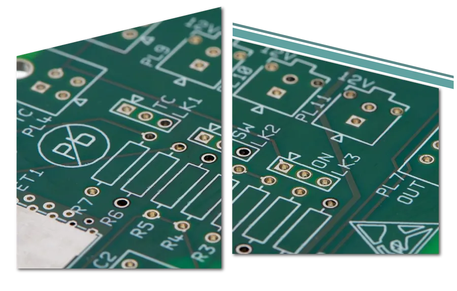
Ordering a PCB prototype for the first time can seem daunting, but with a structured approach, the process becomes straightforward. This guide breaks down the key steps involved, from preparing your design files to tracking your order, ensuring a smooth transition from concept to physical prototype.
It is often helpful to take screenshots of the various stages of your online order with the chosen manufacturing partner. This is useful for both reference, and also to aid in communication with the manufacturer should a problem arise. Below are example screenshots. (Note, these are examples only, and are not intended to be actual representations of a specific manufacturer’s platform).
Desktop PCB printers, such as the Voltera V-One, offer an alternative approach to traditional PCB prototyping, enabling engineers to rapidly iterate on designs in-house. While they present advantages in terms of speed and convenience, it's essential to understand their limitations compared to conventional manufacturing processes.
| Feature | Desktop PCB Printers | Traditional PCB Manufacturing |
|---|---|---|
| Cost | Higher initial investment; lower cost per board for very small runs | Lower initial investment; lower cost per board at medium to large quantities |
| Turnaround Time | Very fast (hours) | Slower (days/weeks) |
| Precision | Lower, often limited to two layers, larger trace width and spacing | High precision, multi-layer capabilities, fine pitch components |
| Materials | Limited to conductive inks and substrates compatible with the printer | Wider range of materials, such as FR4, Aluminum, Flexible substrates |
| Volume | Ideal for very low-volume, internal prototyping | Best suited for medium to high volume manufacturing |
| Complexity | Limited to less complex designs, typically simpler two-layer boards | Supports complex multi-layer designs |
For low-volume, internal prototype testing, a desktop printer may be a suitable option. However, it's important to evaluate your design requirements, including layer count, component size, and feature resolution, to ascertain whether a desktop printer can meet your requirements or if traditional PCB manufacturing services are more appropriate.
This section addresses common queries regarding PCB prototypes, providing clear and concise answers to assist users in understanding their purpose, cost implications, and practical applications in electronic design.
Rapid and cost-effective PCB prototyping is no longer a barrier to innovation. With options ranging from quick-turn manufacturers to desktop printers, today’s electronics engineers and hobbyists have unprecedented access to tools that bring their designs to life. By carefully evaluating project needs, choosing the right service, and preparing designs diligently, you too can swiftly and successfully bring your ideas from concept to functional [pcb prototype] and iterate toward production-ready hardware.

