In the intricate world of electronics, where circuits power our modern lives, the reliability of printed circuit boards (PCBs) is paramount. Enter IPC 2221, a cornerstone standard in the electronics industry. Like the precise measurements that build a skyscraper, IPC 2221 provides the foundational guidelines for PCB design, ensuring that every component, trace, and material choice contributes to a robust and functional end product. This article will be your guide to navigating the critical aspects of this standard.
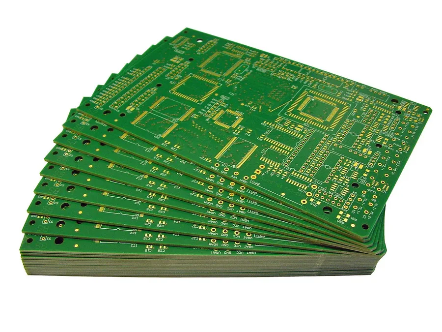
IPC 2221, a foundational document in the IPC-2220 series, establishes the generic requirements for the design of printed circuit boards (PCBs). It is essential for engineers and designers as the primary reference for broad design specifications, impacting subsequent standards in the series. Its application ensures a baseline for consistent, reliable PCB design across various applications.
Specifically, IPC-2221 defines standards and guidelines for material selection, component placement, spacing, trace widths, and clearance calculation, all critical for proper PCB functionality. It serves as the starting point for creating more specific design criteria and is considered a prerequisite for other standards.
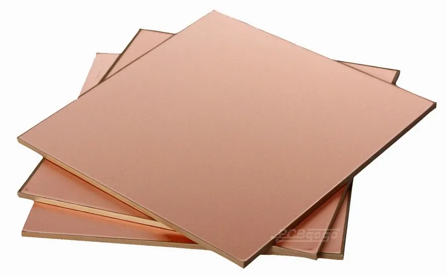
IPC 2221 establishes crucial guidelines for material selection in printed circuit board (PCB) design, ensuring that chosen materials meet the required performance and reliability criteria. This standard emphasizes the impact of material properties—such as conductivity, dielectric constant, and thermal stability—on the overall functionality and lifespan of the PCB.
| Material Property | Impact on PCB Performance | IPC 2221 Considerations |
|---|---|---|
| Dielectric Constant | Influences signal speed and impedance | Specifies acceptable ranges based on application needs |
| Copper Conductivity | Affects current carrying capacity and signal loss | Provides guidelines for trace width and copper thickness |
| Thermal Conductivity | Impacts heat dissipation | Specifies materials based on thermal management requirements |
| Coefficient of Thermal Expansion (CTE) | Leads to stress and potential failures during thermal cycling | Considerations for ensuring compatibility of different materials |
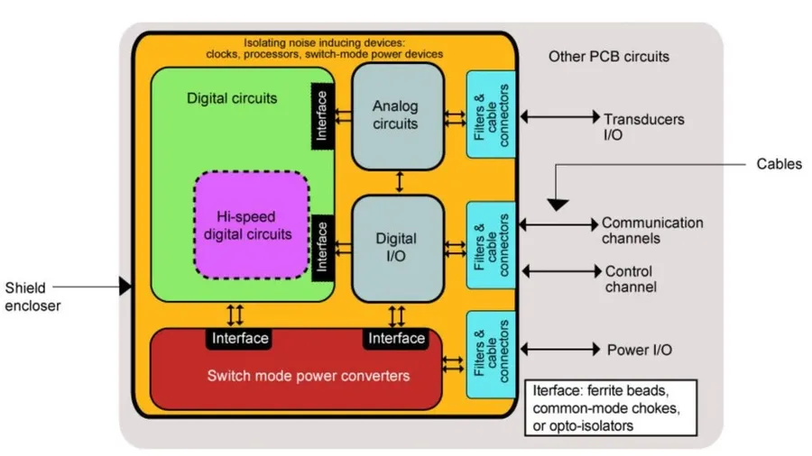
IPC 2221 provides crucial guidelines for component placement on printed circuit boards (PCBs), emphasizing thermal management and signal integrity to ensure optimal functionality. Proper component arrangement is not merely about physical layout; it significantly impacts the performance, reliability, and longevity of the PCB and the overall electronic product.
| Consideration | Description | Impact |
|---|---|---|
| Thermal Management | Placement of heat-generating components for optimal heat dissipation | Prevents overheating and component failure |
| Signal Integrity | Minimizing trace lengths and impedance mismatches | Reduces signal noise and degradation |
| Proximity Rules | Maintaining minimum spacing between components and edges | Prevents electrical shorts and improves manufacturability |
| Test Point Accessibility | Strategic positioning of test points | Facilitates easier testing and debugging |
| Component Orientation | Alignment with signal flow and assembly process | Simplifies assembly and testing |
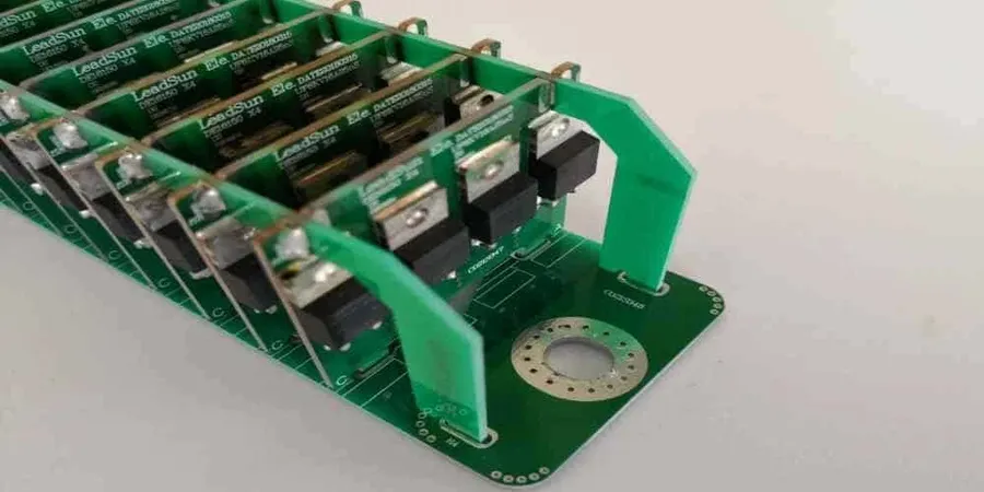
IPC 2221 establishes critical high-voltage spacing requirements to mitigate electrical arcing and ensure the safety and reliability of printed circuit board (PCB) designs. These standards are paramount in preventing short circuits and dielectric breakdown, particularly in applications involving high voltages.
The standard provides specific guidelines on minimum spacing based on factors such as the voltage level, the environment, and the materials used, ensuring compliance with safety regulations and preventing failures. The use of calculators, as detailed below, facilitates the accurate application of these guidelines to real-world designs.
Key Parameters for High-Voltage Spacing:
Importance of Calculators: While IPC 2221 provides the foundational guidelines, engineers often use calculators to implement these guidelines effectively. These calculators help with the determination of creepage and clearance distances based on the specific application requirements. They take into account environmental conditions, material properties, and voltage levels. The calculators allow for accurate and repeatable results, reducing errors and ensuring safety.
| Aspect | Description |
|---|---|
| Creepage Distance | The shortest distance between two conductive parts measured along the surface of the insulating material. |
| Clearance Distance | The shortest distance through air between two conductive parts. |
| Calculation Parameters | Calculations take into account pollution degree, material group, and working voltage to determine appropriate distances. |
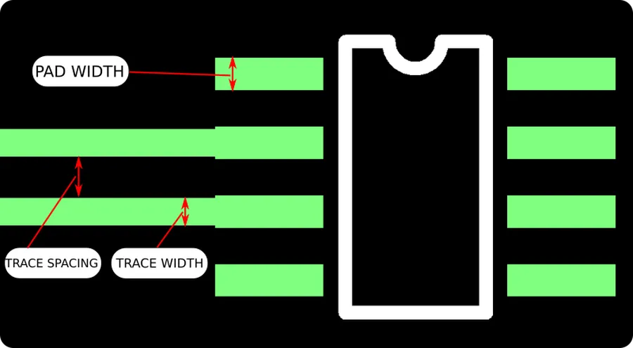
IPC 2221 provides fundamental guidelines for determining trace width limits on PCBs, ensuring they can handle the intended current without excessive heat generation. This standard serves as a crucial reference for preventing thermal issues and guaranteeing reliable power transmission across various PCB designs.
The standard does not directly specify trace widths for particular current values. Instead, it outlines a methodology and factors to be considered when calculating current-carrying capacity (ampacity), which is the maximum current a trace can handle before its temperature rises to an unacceptable level. The key elements to consider include:
While IPC 2221 does not provide specific formulas for trace width, the standard provides guidelines to calculate the necessary cross-sectional area based on the desired current capacity, maximum temperature rise, and the material properties. PCB design tools often incorporate models based on IPC 2221 guidelines, enabling designers to determine appropriate trace widths efficiently.
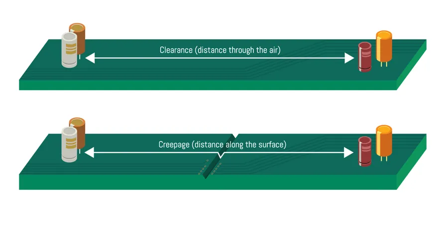
IPC 2221 provides the foundational guidelines for calculating clearances on printed circuit boards (PCBs). These clearances, which are the distances between conductive elements, are critical to prevent electrical arcing, shorts, and other failures, especially in high-voltage applications. Utilizing clearance calculators, as detailed within the standard, is essential for ensuring reliable and safe PCB designs. Proper application of these calculations is not just about meeting minimum requirements; it's about robust design that will perform under a variety of operating conditions.
| Factor | Description | Impact on Clearance |
|---|---|---|
| Voltage | Higher voltages require larger clearances to prevent arcing. | Directly proportional: Higher voltage means larger clearance needed. |
| Altitude | Higher altitudes reduce air density, decreasing the dielectric strength of air, requiring larger clearances to prevent arcing. | Inversely proportional: Higher altitude means larger clearance needed. |
| Pollution Degree | Higher levels of contamination reduce the surface insulation resistance, necessitating larger clearances. | Directly proportional: Higher pollution degree means larger clearance needed. |
| Material Type | The dielectric strength of the PCB material influences required clearance. | Varies based on the material's inherent dielectric properties. Some materials require less clearance than others. |
| Environmental Conditions | Temperature and humidity can affect the dielectric properties and surface resistance requiring increased clearance. | Varied: Specific conditions can require adjusted clearance. |
Clearance calculators, often software-based, use these factors to accurately compute the necessary distances between traces, pads, and other conductive features. These tools are invaluable in high-voltage design scenarios or in situations where specific environmental factors are at play, ensuring that PCB designs remain robust and reliable.
While both IPC 2221 and IPC 2152 are crucial standards in PCB design, they address current-carrying capacity and thermal analysis from different perspectives. IPC 2221 serves as a foundational, generic standard, providing a broad range of guidelines, while IPC 2152 is a more specific standard focused on detailed current-carrying capacity calculations and thermal considerations.
| Feature | IPC 2221 | IPC 2152 |
|---|---|---|
| Scope | Generic PCB design requirements; provides broad guidelines | Specific guidelines for current-carrying capacity and thermal analysis |
| Current-Carrying Capacity | Provides basic formulas and graphs for estimating trace width and current capacity. | Utilizes detailed modeling and calculations for precise current carrying capacity and temperature rise predictions based on environmental factors. |
| Thermal Analysis | Offers general recommendations for thermal management. | Focuses on detailed thermal analysis and considers various parameters, like ambient temperature, trace dimensions, and copper thickness. |
| Complexity | Simpler, more conservative approach. | More complex, requiring advanced simulation tools and data for accurate predictions. |
| Application | Suitable for general PCB design and less demanding applications. | Ideal for high-density, high-power PCBs where precise thermal management and current limits are crucial. |
| Data Basis | Based on empirical data and testing with limitations. | Uses advanced modeling techniques and detailed thermal analysis. |
In practice, IPC 2221 is often used in the initial stages of design or in less demanding applications where a general approach suffices. In contrast, IPC 2152 is employed in scenarios requiring precise current-carrying capacity calculations and detailed thermal analysis to ensure operational reliability and prevent overheating. IPC 2152 is particularly beneficial for high-power, high-density, and thermally demanding applications.
This section addresses common queries regarding the IPC 2221 standard, offering clarity on its core rules, clearance requirements, and distinctions from related standards like IPC 2152.
IPC 2221 serves as the bedrock for robust and reliable PCB design. By adhering to its guidelines, designers ensure that electronic devices perform optimally and safely. From material selection and component placement to high-voltage spacing and trace width, IPC 2221 impacts every facet of PCB design. Embracing this standard ensures that designs are not only functional but also adhere to industry best practices, while also laying the groundwork for ongoing innovation in electronics manufacturing. Understanding IPC 2221 is not just about compliance; it's about building better, more durable technology. This foundational knowledge allows for further exploration and application of specialized standards within the IPC-2220 series.

