In the intricate world of PCB design, the IPC 7351 standard stands as a cornerstone for ensuring the reliability and efficiency of electronic assemblies. Just as a well-fitted shoe is crucial for comfortable walking, accurate component footprints defined by IPC 7351 are essential for successful soldering and long-lasting performance. This article delves into the core principles of IPC 7351, offering a comprehensive understanding to both novice and seasoned designers, bridging the gap between theoretical specifications and practical application.
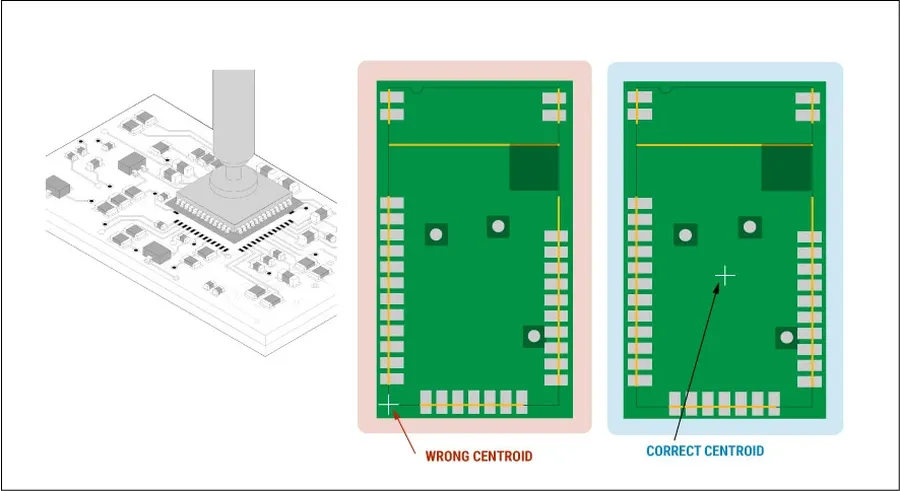
The IPC 7351 standard is a cornerstone in the realm of printed circuit board (PCB) design, specifically addressing the creation of surface mount component footprints. It establishes a uniform system for designing land patterns, ensuring compatibility between components and PCBs. This standardization is critical for consistent, reliable, and repeatable PCB assembly, thereby minimizing errors and optimizing manufacturing processes.
The primary intent of IPC 7351 is to provide a comprehensive set of guidelines that ensure the correct component placement and reliable soldering in surface mount technology (SMT). By adhering to these guidelines, engineers can confidently design PCBs that meet the stringent requirements of modern electronic assembly, minimizing rework and improving the overall efficiency of the production line.
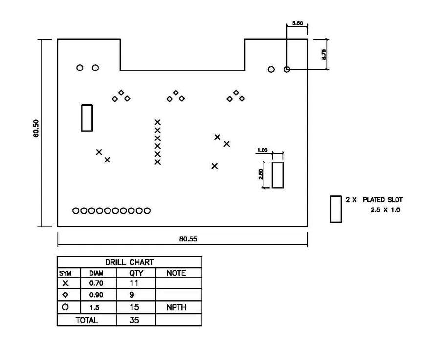
The IPC 7351 standard meticulously defines critical dimensions and tolerances for surface mount component land patterns, ensuring consistent and reliable PCB assembly. These specifications directly influence the solder joint quality, component placement accuracy, and overall product performance. Understanding these parameters is paramount for any PCB designer striving for high-yield manufacturing.
| Parameter | Description | Impact on Land Pattern |
|---|---|---|
| Pad Width (X) | The dimension of the pad along the component's width. This dimension is crucial for establishing proper solder fillet formation and joint strength. | Directly affects the solderable area, impacting solder joint reliability and thermal dissipation. |
| Pad Length (Y) | The dimension of the pad along the component's length. It is essential for creating sufficient solder connection and preventing tombstoning. | Determines the area for solder paste application and the surface area for the solder connection. Insufficient length can lead to poor mechanical and electrical connections. |
| Pad Spacing (G) | The distance between adjacent pads, both within a component footprint and between components. This is crucial for preventing solder bridging and ensuring proper electrical isolation. | A critical factor in preventing solder bridges and ensuring reliable assembly process. Incorrect spacing can lead to shorts or other manufacturing defects. |
| Component Body Dimensions | The physical dimensions of the component itself (length, width, height), This dictates the overall space a component occupies and plays a critical role in determining the size and arrangement of the footprint. | Used in conjunction with the pad dimensions to calculate the full footprint size and spacing. These measurements are vital for design integrity and prevent mechanical interference. |
| Tolerances | Allowable variations in the specified dimensions. These ensure that components and PCB land patterns fit together correctly even with normal variations in manufacturing. | Specifies the permissible deviation from ideal dimensions, impacting the tolerance windows of assembly processes. Careful consideration of these values prevents poor fit between component and land pattern. |
It is paramount that PCB designers carefully adhere to the IPC 7351 specified values to achieve the desired level of manufacturing and assembly reliability. Deviation from the standard may lead to increased defects, lower yields and, ultimately, unreliable products.
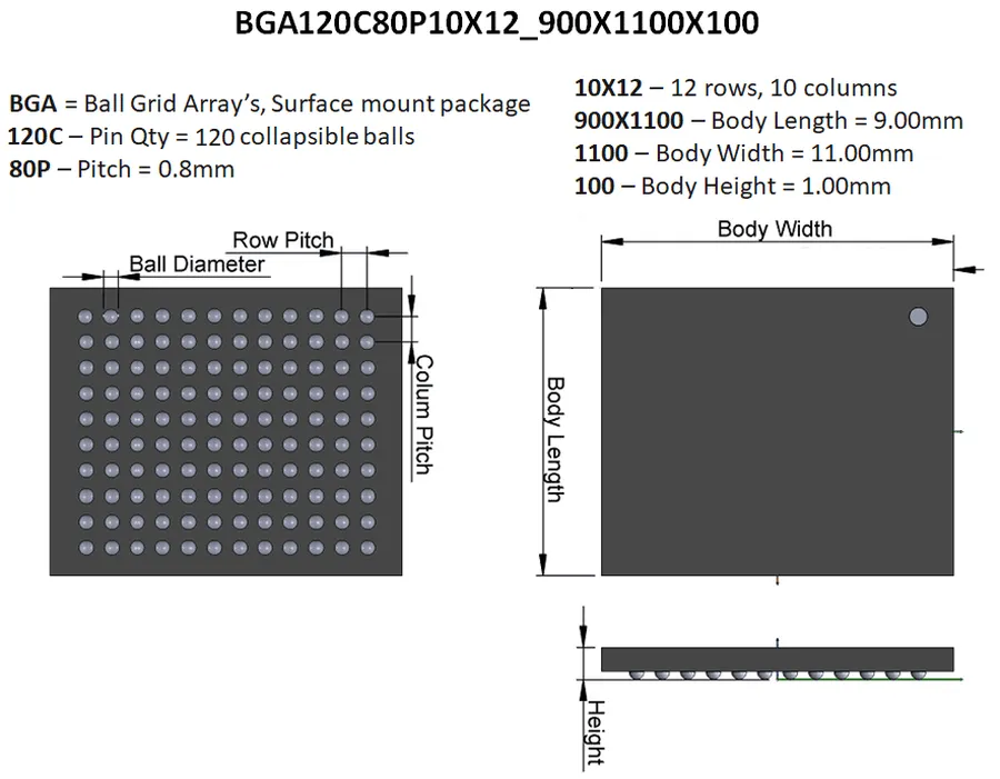
The IPC 7351 naming convention provides a standardized method for identifying component package dimensions and their corresponding land patterns, crucial for effective PCB design and component library management. Understanding this nomenclature is essential for ensuring accurate component selection and placement.
The convention primarily focuses on encoding key physical characteristics of the component and its associated land pattern within a concise alphanumeric string. This reduces ambiguity and potential errors during the design process. The structure is generally consistent, but there can be variations based on the component type and complexity, typically following the format: [Component Type]-[Package Type]-[Dimensions]-[Land Pattern Modifier].
For example, a common naming structure begins with the component type (e.g., R for resistor, C for capacitor, IC for integrated circuit) followed by the package type and dimensions. The dimensions are typically represented in millimeters or inches. Land Pattern Modifiers indicate whether a land pattern is nominal, maximum, or minimum.
| Element | Description | Example |
|---|---|---|
| Component Type | Letter indicating component family | R (Resistor), C (Capacitor), IC (Integrated Circuit) |
| Package Type | Code for package style | SOT, SOIC, QFN, BGA |
| Dimensions | Numerical values for dimensions | 0603 (0.06" x 0.03"), 1206 (0.12" x 0.06"), 1.0x1.2mm |
| Land Pattern Modifier | Suffix indicating density level | N (Nominal), L (Minimum), M (Maximum) |
Interpretation of land pattern designations is straightforward once the naming convention is understood. An 'N' modifier usually indicates a nominal land pattern, which represents a design target within the tolerance limits. 'L' and 'M' often indicate minimum and maximum land pattern dimensions. These modifiers are particularly useful when accounting for variations in manufacturing and assembly.
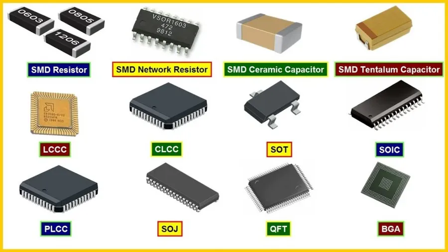
The IPC 7351 standard is fundamentally intertwined with Surface Mount Technology (SMT). SMT, which involves mounting electronic components directly onto the surface of a printed circuit board (PCB), presents unique challenges in component placement and soldering. IPC 7351 provides standardized land pattern dimensions and tolerances specifically designed to address these challenges, ensuring reliable automated assembly processes and high-quality solder joints.
By adhering to IPC 7351 guidelines, PCB designers can create footprints that optimize the following key aspects of SMT assembly:
The standard takes into consideration the various SMT processes, such as reflow soldering, and different pad designs suitable for these processes. It provides essential guidance for land pattern design that minimizes defects common in SMT. This is achieved through recommendations for various parameters, including pad size, shape, and the spacing between pads, all of which play a pivotal role in ensuring proper solder joint formation and avoiding common defects. Proper design according to IPC 7351 is crucial for ensuring high-yield manufacturing, reducing rework, and achieving overall product reliability.
| SMT Challenge | IPC 7351 Solution | Resulting Benefit |
|---|---|---|
| Component Misalignment | Standardized land patterns with precise pad dimensions | Improved placement accuracy by automated machines |
| Insufficient solder joint strength | Land pattern sizes to ensure adequate solder volume | Robust and reliable solder joints |
| Solder defects (Tombstoning, bridging) | Controlled pad dimensions and spacing | Minimized manufacturing defects |
| Inconsistent assembly process | Uniform footprint design within package types | Streamlined SMT process with reduced setup time |
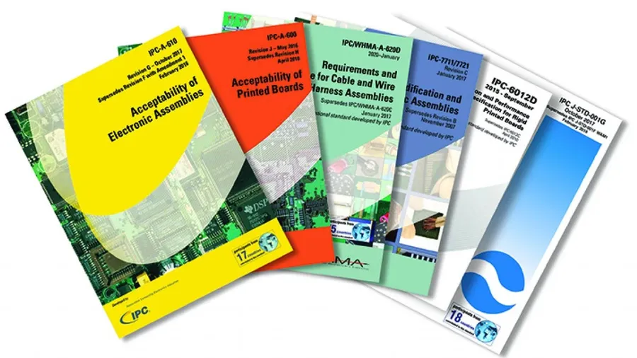
The IPC 7351 standard represents a significant advancement in PCB footprint design, superseding earlier methodologies and setting the stage for future revisions. It refines the process of creating land patterns for surface mount components, enhancing assembly reliability and consistency. Understanding its evolution and relationship to other standards like IPC-7352 is crucial for PCB designers.
| Feature | IPC-SM-782 | IPC 7351 | IPC-7352 |
|---|---|---|---|
| Primary Focus | General land pattern guidelines. | Detailed component footprint design. | Component mounting and physical outline standard |
| Scope | Less prescriptive, allowing variation. | Highly prescriptive and specific. | Dimensional and mounting guidelines for electronic components |
| Pad Dimensions | Variability in pad size calculation | Standardized formulas for calculating X, Y, and G dimensions. | Covers detailed body dimensions and mounting pad locations. |
| Nomenclature | Less detailed naming conventions. | Rigorous component and land pattern naming convention. | Comprehensive naming system for component physical attributes |
| Application | Used as basis for older footprint design | Widely adopted for current SMT design. | A good standard to consult for component mounting and physical attributes. |
| Relationship to IPC 7351 | Precursor to 7351 | Builds upon 782 to enhance footprint accuracy. | Provides related component and mounting standards. |
| Relationship to IPC 7352 | No direct relationship | Interoperable with IPC-7352 to streamline design. | Addresses physical component outline and mounting requirements that can be used with IPC-7351. |
The discussion around a potential 'IPC-7351C' is largely speculative as of the last update, with no official standard released by IPC. However, it is important to stay informed of potential changes or updates to the standard from official sources. While IPC-7351 concentrates on the footprint design, IPC-7352 provides component mounting and physical outline standards. IPC-7351 and IPC-7352 are complementary to each other. The former focuses on how the footprint should be made, while the latter focuses on the components physical dimensions. Both work together to ensure that a component can be properly mounted to the PCB.
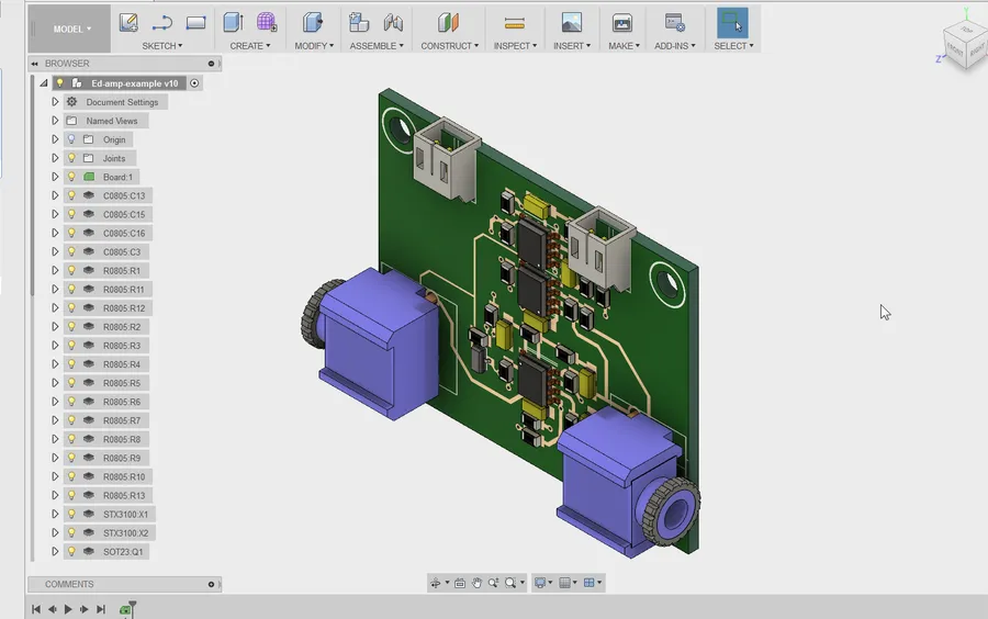
Integrating IPC 7351 guidelines within PCB design software is crucial for ensuring the accuracy and reliability of PCB designs. This section outlines the process of effectively utilizing these standards within common design tools to streamline footprint creation, verify compliance, and enhance the overall design workflow.
| Feature | Description | Benefits |
|---|---|---|
| Component Libraries | Manage and store IPC 7351 compliant component footprints. | Ensures consistent use of standardized footprints, reducing errors. |
| Footprint Creation Tools | Automate generation of land patterns based on IPC 7351 specifications. | Reduces design time and minimizes human error. |
| Design Rule Checks | Set rules based on IPC 7351 standards for spacing, clearances. | Ensures design compliance and eliminates errors in manufacturing. |
| Data Import/Export | Share IPC 7351 data between different software platforms. | Facilitates collaboration, ensures consistent designs across platforms. |
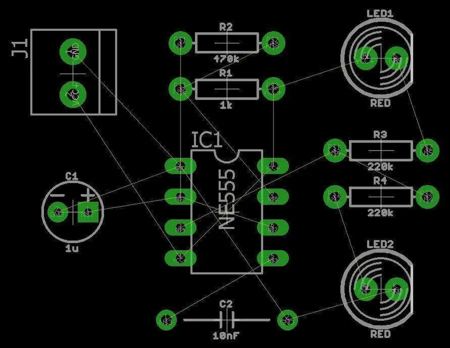
IPC 7351 significantly impacts component orientation on a Printed Circuit Board (PCB) to ensure accurate and reliable assembly and optimal functional performance. Consistent component placement, guided by this standard, is crucial for automated assembly processes and minimizing potential errors.
The standard not only dictates the land pattern but also implicitly guides the preferred orientation of components. While IPC 7351 doesn't explicitly define component orientation rules, the underlying land pattern design influences how components must be placed to align with the footprint. For instance, polarized components like capacitors and diodes have specific orientation markings that must align with the PCB footprint, and IPC-7351 compliant land patterns are designed with this in mind.
Consistent orientation across a board simplifies automated assembly, reduces human error, and minimizes rework. Incorrect orientation can result in electrical malfunctions, damage to components, and board failures. Therefore, when designing PCB layouts and selecting components, engineers must consider orientation within the constraints of the IPC 7351 standard to achieve optimal board functionality and assembly efficiency.
This section addresses common queries regarding the IPC 7351 standard, providing clear and concise answers to help clarify its purpose and application in PCB design. Understanding these FAQs is crucial for effectively implementing IPC 7351 guidelines.

Leveraging the IPC 7351 standard effectively is crucial for achieving optimal PCB design, encompassing component selection, footprint design, and overall manufacturability. A thorough understanding of IPC 7351 allows designers to make informed decisions that directly impact the reliability and performance of the final product. By adhering to the standard, the risk of assembly errors and failures is significantly reduced.
By applying IPC 7351 standards, PCB designers not only streamline the manufacturing process, but also enhance product reliability and performance. This approach ensures that the final product meets the intended specifications and reduces the risk of failures.
Adhering to the IPC 7351 standard is not merely about following rules; it's about ensuring that every component, from the smallest resistor to the most complex IC, sits precisely where it needs to be for optimal performance. As technology evolves, staying updated with the latest in IPC 7351 and its subsequent versions is crucial for any PCB designer striving to create robust and reliable electronic products. By understanding and implementing these standards, the industry can achieve greater consistency, accuracy, and ultimately, better electronics. The future of PCB design rests on the precise foundation of standards like IPC 7351.

