Mastering PCB Layout Design: A Comprehensive Guide
2025.02.01
In today's fast-paced technology landscape, Printed Circuit Boards (PCBs) are the backbone of nearly every electronic device. The layout design of a PCB is a critical step that determines the functionality and reliability of the final product. Like a blueprint for a city, a well-planned PCB layout ensures smooth and efficient operations, preventing issues that might lead to costly failures. This article will serve as a complete guide, exploring the various aspects of PCB layout design, offering insights that enhance your understanding and execution of this essential engineering task, as well as guiding you through the process of selecting the right PCB design tools.
Understanding the Fundamentals of PCB Layout Design
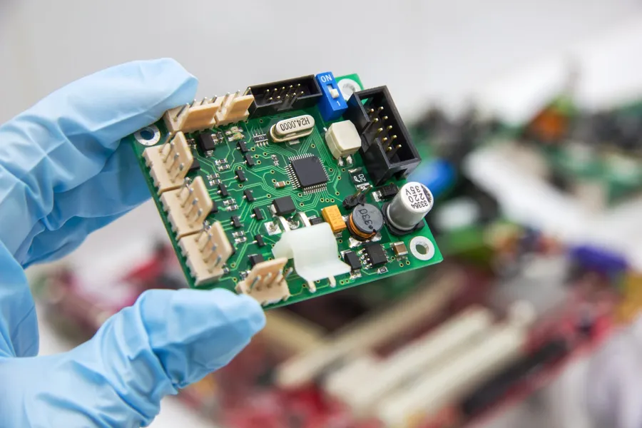
Printed Circuit Board
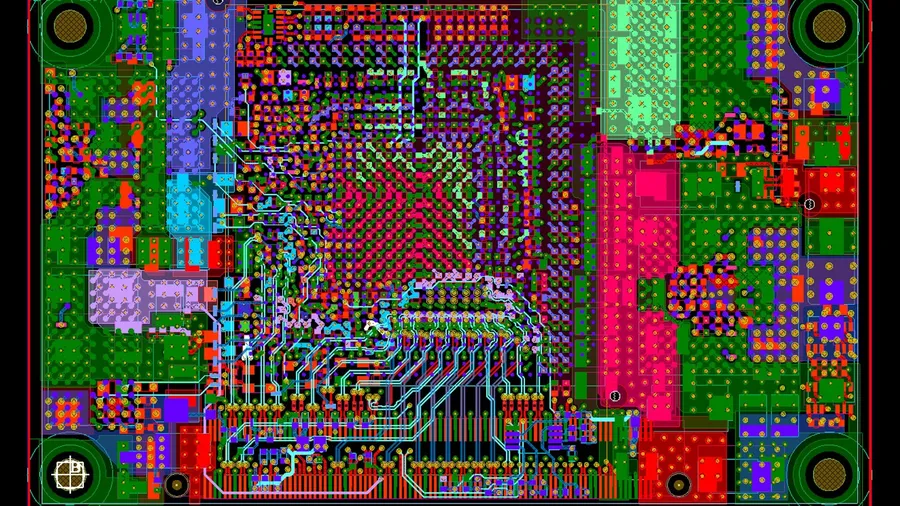
At its core, PCB layout design is the art and science of arranging electronic components and their conductive pathways on a printed circuit board (PCB). This process is pivotal in transforming a schematic diagram into a physical, functioning electronic product. A well-executed PCB layout is not merely about connecting components; it's about optimizing for performance, reliability, manufacturability, and cost. The physical arrangement directly impacts signal integrity, thermal management, and the overall efficacy of the electronic device.
Key aspects of PCB layout design include:
Component Placement Strategic arrangement of components based on their functionality, thermal requirements, and signal flow. Poor placement can lead to routing complexities and performance degradation.
Signal Routing Creating conductive pathways for signals to travel between components. This involves careful consideration of trace width, impedance, and isolation to ensure signal integrity and prevent interference.
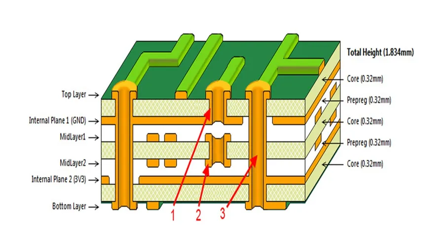
Layer Stack-up The arrangement of copper and dielectric layers in a multi-layer PCB which significantly influences signal integrity, EMI, and power distribution.
Grounding and Power Distribution Developing a robust and low-impedance power and ground networks, which is critical for ensuring stable operation, and minimizing noise.
Design Rule Checks (DRC) Using software to verify adherence to design rules, such as trace spacing, via sizes, and clearances. This helps to prevent manufacturing errors and functional defects.
Effective PCB layout design is a balance between electrical engineering principles and practical manufacturing constraints. It is an iterative process that requires careful planning, execution, and verification, ultimately ensuring the circuit board performs as intended within the desired specifications.
Essential Steps in PCB Layout Design
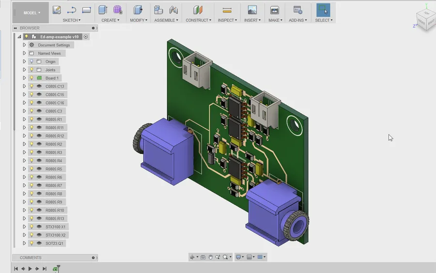
PCB Design Software
Effective PCB layout design requires a systematic approach, transforming a schematic diagram into a physical circuit board. This process, from initial setup to final cleanup, dictates the performance and reliability of the electronic device. The key stages include setting up the design environment, defining the board outline, importing the netlist, meticulously placing components, skillfully routing signals, and concluding with a comprehensive silkscreen review. Each stage demands precision and a deep understanding of electronic principles to ensure a successful board design.
Setting Up the Design Environment The first crucial step involves configuring the PCB layout software. This includes setting design rules, specifying layer stack-ups, and configuring units of measure. Proper setup from the outset prevents errors and ensures compatibility with manufacturing processes.
Defining the Board Outline Precisely defining the physical dimensions and shape of the PCB is paramount. This outline determines the available space for components and traces. Considerations must include enclosure compatibility and manufacturing limitations.
Netlist Import The netlist, generated from the schematic design, serves as the blueprint for connections. Importing this netlist into the layout software ensures that the intended electrical connectivity is accurately implemented on the physical board.
Component Placement Strategic component placement is essential for signal integrity, thermal management, and ease of assembly. Components must be arranged logically, considering signal flow and physical constraints. This includes grouping related components and paying attention to critical placement requirements.
Signal Routing Routing involves creating conductive paths between components according to the netlist. This step demands precise control of trace impedance, length, and spacing. Special attention is needed for sensitive signals and high-speed traces.
Silkscreen Cleanup The final step involves reviewing and cleaning up the silkscreen layer, ensuring all necessary text, component designators, and logos are readable and correctly positioned. This facilitates assembly, maintenance and general usability of the board.
Component Placement Strategies
PCB Component Placement
Effective component placement on a PCB is paramount for achieving optimal performance, signal integrity, and manufacturability. This involves strategic positioning of components while considering thermal management, signal path lengths, and ease of assembly. Proper planning during this stage significantly reduces routing complexity and ensures the long-term reliability of the final product.
Thermal Considerations: High-power components should be placed to facilitate heat dissipation, often near the edges of the board or heat sinks. Group heat-generating components to allow for centralized thermal management solutions. Avoid placing temperature-sensitive components near heat sources.
Signal Integrity: Place components such that critical signal paths are as short as possible to minimize signal reflections and EMI. Consider the placement of high-speed components close to their supporting circuitry. Group components involved in the same signal path to prevent lengthy traces.
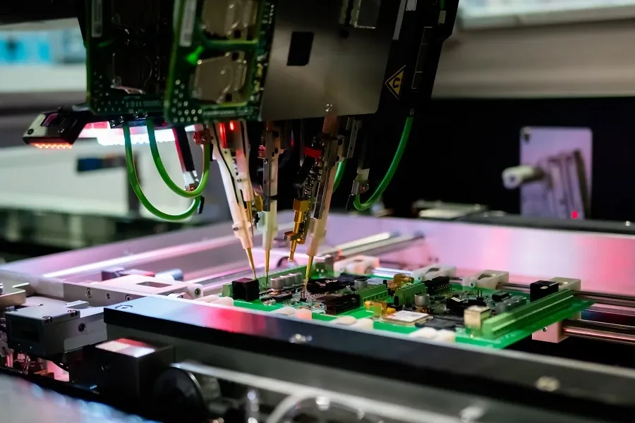
Ease of Assembly: Arrange components to ensure that automated assembly processes can be followed without obstruction, and test points are easily accessible. Place similar component types and sizes together to streamline assembly procedures, and consider that the orientation of polarized components should be consistent to prevent errors.Ensure sufficient spacing between components for pick and place machinery.
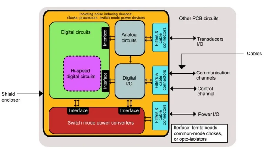
Analog and Digital Separation: Keep analog and digital components physically separated on the board. Analog circuits are sensitive to noise, therefore should be located away from noisy digital circuits. This placement also reduces the chance of interference and improves circuit performance.
Decoupling Capacitors: Position decoupling capacitors very close to the power pins of the ICs to minimize voltage transients. They provide localized power, thus reducing the need for a large power delivery network.
Component Type
Placement Strategy
Rationale
Microcontrollers/Processors
Central location, close to memory and peripherals
Minimizes signal path lengths and facilitates interconnectivity
Memory Chips
Adjacent to the processor, with short traces
Reduces latency and maximizes data transfer efficiency
Power Supplies
Near the board edge or heat sinks, with dedicated heat dissipation solutions
Enables proper thermal management and reduces interference
Connectors
Along board edges, with consideration to user interaction and enclosure
Allows easy access and simplifies enclosure integration
Analog Components
Separated from digital sections, with adequate grounding
Reduces noise and ensures signal integrity
Signal Routing Techniques
PCB Trace Routing
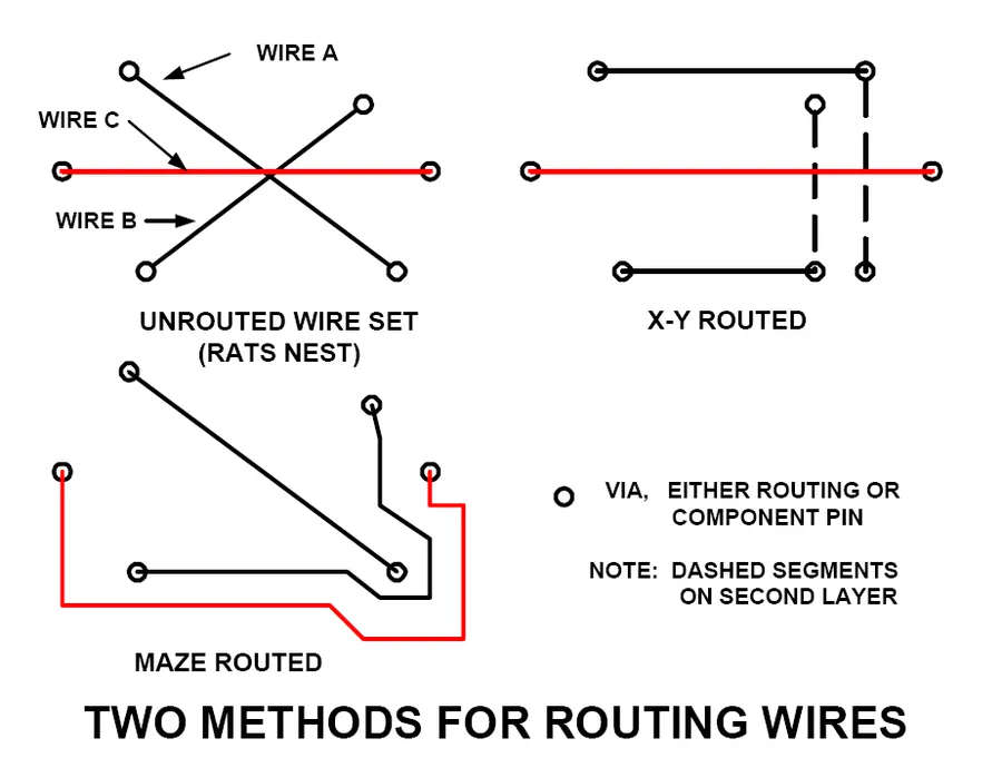
Efficient signal routing is paramount in PCB layout design, directly influencing signal integrity and overall circuit performance. This involves carefully planning the paths that electrical signals take across the board, encompassing both manual and automated routing approaches to manage signal behavior, particularly for high-speed signals, and ensuring impedance matching.
Key considerations include controlling impedance to minimize reflections, carefully routing differential pairs to reduce noise, and accurately calculating trace widths to handle current flow without causing excessive voltage drops. This section provides a detailed look at these critical aspects of signal routing.
Routing Technique
Description
Advantages
Disadvantages
Manual Routing
Designers route traces individually based on their knowledge and the specific requirements of the design.
High level of control, optimized for complex designs, allows for the implementation of specific design strategies.
More time consuming, requires significant design expertise, can be prone to human error.
Autorouting
Software algorithms route the traces automatically according to predefined rules and constraints.
Faster routing, can be useful for simple and low-density designs, easy to use, can handle large design.
Potentially lower quality routes, less optimization, may need manual adjustment, requires good setup of routing rules.
Differential Pair Routing
Routing two traces carrying differential signals with equal length, impedance and spacing.
Reduces noise, minimizes electromagnetic interference, essential for high-speed signals, improves signal integrity.
Requires careful planning, can be complex in dense designs, may increase routing congestion.
Impedance Matching
Adjusting trace width and spacing to achieve a specific impedance value, often 50 ohms.
Prevents signal reflections, minimizes signal loss, ensures proper signal transfer, optimizes signal performance.
Requires precise calculation, may be hard to achieve in complex designs, can increase routing area.
PCB Design Guidelines for Engineers
PCB Engineer Workstation
Adhering to established PCB design guidelines is paramount for engineers to ensure the functionality, reliability, and manufacturability of circuit boards. These guidelines serve to prevent common errors, minimize signal interference, and optimize overall performance, ultimately leading to a robust and efficient final product. They address crucial aspects such as trace spacing, via placement, component clearances, and more.
Trace Spacing Maintaining adequate spacing between traces is crucial to prevent shorts and crosstalk. The required spacing is often determined by the voltage difference between adjacent traces and the PCB's manufacturing capabilities. IPC-2221 provides minimum spacing guidelines based on voltage levels and environmental conditions. For instance, higher voltage circuits necessitate greater spacing. Also, differential signals require specific spacing rules to maintain impedance.
Via Placement Vias are used to connect traces on different layers of the PCB. They should be placed strategically to minimize signal path length and impedance mismatches. Avoid placing vias within sensitive signal paths or too close to high-current carrying traces, to reduce signal integrity and thermal issues. It's also advisable to use multiple vias for high-current traces to lower resistance. For high speed signals, backdrilling may be necessary. Signal vias should be placed as directly as possible to minimize via stubs and maintain controlled impedance.
Component Clearances Adequate clearance around components is vital for assembly, testing, and thermal management. Sufficient space between components prevents assembly issues and enables effective heat dissipation. Follow component manufacturer recommendations for clearances, which includes consideration for manufacturing tolerances and repair access. Different component types may have different clearance requirements. Keep in mind thermal management. Some components will require thermal relief pads which will impact the required spacing.
Ground Plane Considerations A solid ground plane is crucial for minimizing noise and ensuring signal integrity. A continuous ground plane is essential for reducing return path impedance. This plane helps create a low-impedance return path for signals, reducing electromagnetic interference (EMI) and signal distortion. Ensure the ground plane is as large as possible and connect it well with vias. The number of ground vias should be based on signal layer via density. A solid ground plane also provides a low impedance path for thermal energy. Make sure thermal connections are made.
Power Distribution The power distribution network (PDN) is crucial for a stable system. A well-designed PDN should provide stable and clean power to all components. Use wide traces or power planes to minimize voltage drops, and employ decoupling capacitors near each power input to smooth out voltage fluctuations. When placing the decoupling capacitors, be mindful of trace inductance and via inductance. There are numerous power distribution analysis tools to assist in ensuring a good power network.
Guideline
Description
Rationale
Trace Spacing
Maintain adequate separation between conductive paths
Prevents shorts, crosstalk, and signal interference
Via Placement
Strategic positioning of vias for layer transitions
Minimizes signal path length and impedance mismatches
Component Clearances
Ensure sufficient space around components
Facilitates assembly, testing, thermal management, and repairs
Ground Plane
Use a solid ground plane
Minimizes noise, reduces return path impedance, provides a low impedance path for thermal energy
Power Distribution
Implement a stable and reliable power distribution network
Provides stable and clean power to all components and helps with voltage fluctuations
Selecting the Right PCB Layout Software
PCB Design Software UI
Choosing the appropriate PCB layout software is a critical decision that significantly impacts the efficiency and success of any electronic design project. The market offers a variety of tools, each with distinct strengths and weaknesses. This section aims to provide a comparative analysis of some popular options, focusing on key aspects like user interface, routing capabilities, and simulation features to aid in selecting the right tool for your specific needs.
Basic SPICE Simulation, Limited Compared to Commercial Tools
Free
Community-Driven, Growing Functionality, Suitable for Hobbyists and Small Projects
EasyEDA
Web-Based, Easy to Use, Cloud Collaboration
Basic Routing Tools, Sufficient for Standard Designs
Basic Circuit Simulation, Cloud-Based
Free (with Paid Options)
Beginner-Friendly, Cloud-Based Design, Integrated with LCSC Component Marketplace
Frequently Asked Questions About PCB Layout Design
This section addresses common questions that newcomers to PCB layout design often have, providing clear and concise answers to facilitate a better understanding of the subject.
What exactly is PCB layout design? PCB layout design is the process of arranging electronic components and their interconnections on a printed circuit board. It involves translating a schematic diagram into a physical layout that allows the circuit to function as intended. This process is crucial for ensuring the proper electrical performance, signal integrity, and manufacturability of the final product.
How should I organize a PCB layout for optimal performance? Organizing a PCB layout involves several key steps. Begin with a clear understanding of the circuit's functional blocks and their interactions. Group related components, place critical components first (like power supplies and high-speed components), and then organize other components around them. Consider signal flow, minimize track lengths, and ensure sufficient spacing between components and tracks to avoid interference and ensure efficient heat dissipation. Proper layer stack up, including ground planes, plays an important part.
What are the essential guidelines for effective PCB layout design? Effective PCB layout requires adherence to several guidelines. These include maintaining proper trace widths and spacing to manage impedance, using vias appropriately to connect different layers of the board, adhering to thermal management considerations by arranging heat-generating components for optimal heat dissipation, avoiding right-angle bends in traces (45-degree or arc-shaped bends are better), and ensuring adequate clearance around pads and components for manufacturability. A detailed understanding of signal integrity requirements is also critical.
What are the top 3 crucial steps in the PCB design and layout process? The top three critical steps in PCB design and layout include 1) **Schematic capture and netlist generation:** This involves creating the logical representation of the circuit and extracting the necessary connectivity information. 2) **Component Placement:** Carefully arranging components on the board to optimize signal paths, thermal considerations and ease of assembly. 3) **Signal Routing:** Defining the paths for electrical signals to follow on the PCB, aiming for minimal interference and maintaining signal integrity. These steps form the foundation of a well-designed PCB.
What is the importance of a ground plane in PCB design? A ground plane is a conductive layer in a PCB that serves as a common reference point for all signals on the board. Its primary functions include providing a low-impedance path for return currents, minimizing noise and interference, and ensuring consistent signal behavior. A well-designed ground plane is crucial for signal integrity, especially in high-speed and high-frequency circuits.
How does layer stack-up affect PCB performance? The layer stack-up of a PCB refers to the arrangement of conductive layers and insulating materials in a multi-layer board. It significantly impacts signal integrity, impedance control, and noise reduction. A well-planned stack-up can minimize signal crosstalk, provide low impedance paths for power distribution, and optimize signal return paths. The number of layers, type of materials used, and their order must be selected to ensure proper PCB performance.
Advanced PCB Layout Techniques
Multi Layer PCB
Advanced PCB layout techniques are crucial for designs requiring high performance, reliability, and signal integrity. These techniques address specific challenges related to impedance control, thermal management, and high-speed signal routing, going beyond basic layout practices to meet demanding performance criteria. Successful implementation of these methods is essential in complex electronic devices to ensure proper functionality and longevity.
Impedance Control Impedance control is crucial for maintaining signal integrity, especially in high-speed designs. By precisely controlling trace geometry and dielectric properties, we minimize signal reflections and ensure efficient power transfer. This requires accurate calculations and adherence to specific trace widths and spacing.
Thermal Management Effective thermal management is critical for preventing overheating of electronic components. Advanced techniques involve using thermal vias, heat sinks, and strategic component placement to dissipate heat effectively and maintain device reliability and longevity. Proper design ensures the safe operation of devices even at high power.
High-Speed Routing High-speed signal routing involves specialized techniques to minimize signal distortion and maintain signal integrity in demanding applications. Differential pair routing, precise trace length matching, and controlled impedance routing are crucial techniques. This is crucial for technologies like DDR memory and high-speed data transmission systems.
Technique
Description
Application
Impedance Control
Precisely controlling trace dimensions and dielectric properties to ensure consistent signal impedance.
High-speed digital circuits, RF circuits, and communication systems.
Thermal Management
Using thermal vias, heat sinks, and strategic component placement to effectively dissipate heat.
High-power devices, power supplies, and systems operating in harsh environments.
High-Speed Routing
Techniques like differential pair routing, impedance matching, and precise trace length control.
DDR memory interfaces, high-speed data transmission, and high-frequency circuits.
Practical Tips for Efficient PCB Layout Design
PCB Testing
Efficient PCB layout design is crucial for the performance and reliability of electronic products. These practical tips and best practices will help you streamline your design process and avoid common pitfalls, leading to successful projects.
Plan Ahead Thoroughly Before starting the layout, create a detailed plan that includes component placement strategy, signal routing requirements, and critical circuit considerations, minimizing the chance of costly rework.
Maintain Clear Documentation Document each design stage, including component selection, layout decisions, and routing strategies. This ensures that all team members and future engineers have a full understanding of design choices. Proper documentation also facilitates future design iterations.
Prioritize Critical Signal Paths Focus on routing critical signals, like high-speed or sensitive analog lines first. This ensures the best possible signal integrity and minimizes noise coupling, thereby enhancing the performance of the design.
Optimize Component Placement Place components based on their function and interaction with other parts of the circuit. For example, place components that interact directly with each other close to one another. Consider thermal management and physical constraints as well to reduce manufacturing issues.
Utilize Software Features Efficiently Become proficient in using your chosen PCB layout software. Leverage features such as autorouting with caution, design rule checks (DRCs) for design integrity, and netlist validation for accuracy to streamline the layout process and ensure error-free board designs.
Conduct Thorough Design Reviews Always involve other engineers and experts in the design review process. Get opinions and perspectives from others on various aspects of the layout to catch potential issues. This step provides a layer of safety and ensures compliance with best practices.
Adhere to Design Rules Strict adherence to design rules and manufacturer-specific recommendations helps to prevent future issues, thereby saving time and resources. Following these rules ensures that the design is manufacturable and cost-effective.
Regularly Back Up Your Work Regular backups of your project files throughout the design process are essential. This precautionary measure protects against data loss and helps ensure you can pick up where you left off in case of software or system failures.
Mastering PCB layout design is crucial for creating reliable and efficient electronic devices. This comprehensive guide has covered the fundamental steps, best practices, and key considerations for effective PCB design. By understanding these concepts, you can enhance your PCB layout skills, minimize errors, and create high-quality circuit boards that meet all your specifications. Remember, careful planning and attention to detail in your PCB layout design, like the careful planning of a city layout, can make a significant difference in the outcome of your projects and impact the performance of the final product.