The Complete Guide to PCB Designers: Skills, Roles, and Career Paths
2025.01.28
In today's technology-driven world, printed circuit boards (PCBs) are the backbone of virtually every electronic device we use. The creation of these intricate components falls into the hands of skilled PCB designers. This article will delve into the multifaceted role of PCB designers, examining their skills, responsibilities, and the various career paths available in this crucial field. Whether you are a seasoned engineer or aspiring to join this exciting area, understand the crucial role PCB designers play in our technological landscape.
What Exactly Does a PCB Designer Do?
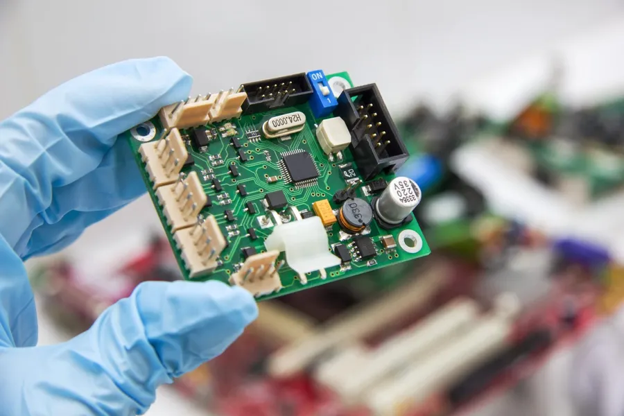
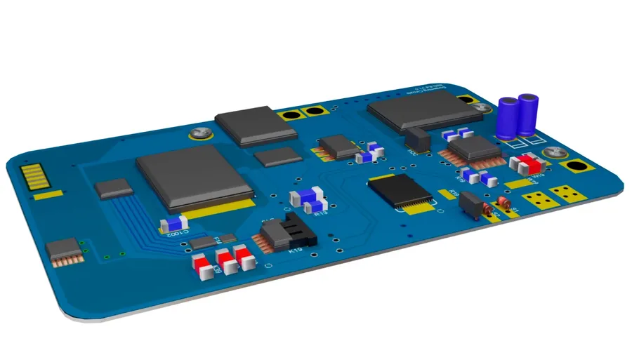
Printed Circuit Board
At the heart of electronics manufacturing, PCB designers translate abstract electronic schematics into tangible physical layouts for printed circuit boards (PCBs). This crucial role involves more than just creating a visual representation; it demands a comprehensive understanding of electrical engineering principles, materials science, and manufacturing processes to ensure functionality, reliability, and cost-effectiveness.
The work of a PCB designer can be understood through a series of key functions, which are essential for successful PCB production:
Schematic Interpretation PCB designers begin by interpreting electronic schematics, which are symbolic representations of electronic circuits, understanding how individual components are connected and their intended functionality within the circuit.
Component Placement This involves strategically positioning components on the PCB layout, taking into account factors such as thermal management, signal integrity, ease of assembly, and the physical dimensions of the components themselves.
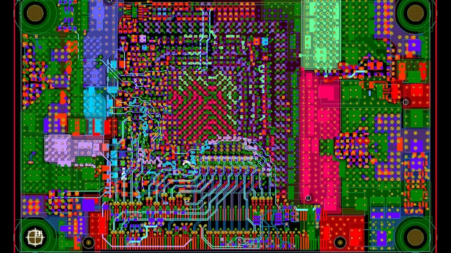
Trace Routing PCB designers create conductive pathways (traces) that connect the various components on the PCB, with careful consideration of impedance matching, signal timing, and minimizing interference or crosstalk.
Design Rule Checks (DRC) Ensuring the design adheres to specific manufacturing guidelines, which are crucial to guarantee the PCB's manufacturability. This includes checks on trace width, spacing, and via sizes.
Thermal Management Employing techniques to manage heat generated by electronic components, such as strategically placed heat sinks or vias to dissipate heat effectively, ensuring the device does not overheat.
Design for Manufacturability (DFM) Considering the limitations of the manufacturing process to ensure that the final PCB can be reliably produced in a cost-effective manner. This often involves collaboration with manufacturers.
Key Responsibilities of PCB Designers
PCB Design Software
PCB designers are pivotal in transforming abstract electronic schematics into tangible printed circuit board layouts. Their responsibilities extend far beyond simple drafting; they encompass critical tasks essential for the functionality, reliability, and manufacturability of electronic devices. These tasks demand a strong grasp of engineering principles, technical proficiency, and problem-solving acumen.
Component Placement Strategic placement of electronic components on the PCB to optimize signal integrity, minimize interference, and ensure efficient heat dissipation. This involves careful consideration of component size, type, and thermal requirements.
Trace Routing Creating conductive pathways (traces) that connect components on the PCB, ensuring proper signal transmission, impedance control, and minimal signal loss. Routing involves meticulous planning of trace width, spacing, and layer assignments.
Layer Management Managing the number of layers in the PCB and assigning signals, power, and ground to appropriate layers to avoid cross-talk and electromagnetic interference.
Thermal Management Designing the PCB layout to dissipate heat efficiently, preventing component overheating and ensuring the device's long-term reliability. This might include the use of thermal vias, heat sinks, and careful component placement.
Design for Manufacturability (DFM) Ensuring that the PCB design can be easily and cost-effectively manufactured, considering factors such as component availability, soldering requirements, panelization, and assembly processes.
Design for Testability (DFT) Integrating test points into the design to facilitate efficient testing and debugging during manufacturing and throughout the product lifecycle.
Signal Integrity Analysis Analyzing the signal quality on the PCB to prevent signal reflections, impedance mismatches, and timing issues by using software simulations.
Generating Gerber Files Producing the necessary manufacturing files, including Gerber files, for PCB fabrication.
Bill of Materials (BOM) Management Creating and managing accurate BOMs for the PCB assembly process.
Essential Skills for PCB Designers
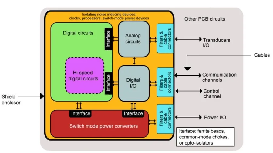
Component Placement
Successful PCB design requires a blend of technical proficiency and interpersonal skills. PCB designers must master both the science of circuit board layout and the art of effective communication, ensuring that designs are not only functional but also manufacturable and meet the project's requirements.
The following skills are crucial for PCB designers:
Proficiency in EDA Software Expertise in Electronic Design Automation (EDA) software is fundamental. This includes using tools for schematic capture, PCB layout, and simulation. Software like Altium Designer, KiCad, and Cadence Allegro are industry standards, and proficiency with at least one is essential. Designers need to use these tools to create accurate and manufacturable designs efficiently.
Understanding of Electrical Engineering Principles A deep understanding of electrical engineering principles is crucial for PCB designers. This encompasses knowledge of circuit theory, signal integrity, power distribution, and impedance matching, enabling them to create efficient and reliable PCB layouts. A strong grasp of these concepts ensures the board functions as intended and meets performance specifications.
Component Knowledge A thorough understanding of electronic components, including their characteristics, footprints, and thermal properties is essential. PCB designers need to be able to select the right components for the application and ensure they are placed correctly on the board to guarantee proper performance and manufacturability.
Problem-Solving Abilities PCB design often involves navigating complex challenges, including optimizing space, managing signal interference, and accommodating thermal constraints. Effective problem-solving is needed to make design decisions that meet all requirements, ensuring the board's functionality, and manufacturability.
Attention to Detail PCB design requires meticulous attention to detail, as even small errors in layout can cause significant issues in the final product. Attention to detail is essential to ensure accurate component placement, proper trace routing, and adherence to design specifications, which guarantees the board's reliability and performance.
Communication Skills Effective communication with other engineers, manufacturers, and project managers is vital for clarifying design requirements, resolving issues, and delivering high-quality designs. PCB designers must be able to convey complex technical details clearly to all stakeholders and ensure that the design aligns with the overall project goals.
Knowledge of Design for Manufacturability (DFM) Understanding DFM principles is essential to design boards that are both functional and easy to manufacture. This includes understanding manufacturing processes, tolerances, and constraints. A good knowledge of DFM reduces manufacturing costs and ensures high-quality end products, ultimately saving time and resources.
Choosing the Right PCB Design Software
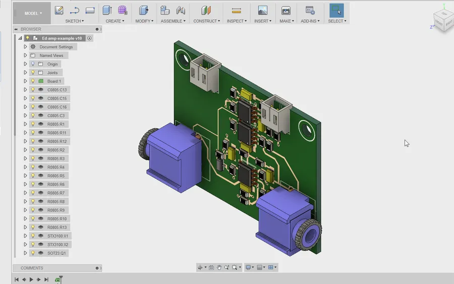
PCB Design Software Options
Selecting the appropriate PCB design software is a critical decision for any PCB designer, as it directly impacts efficiency, accuracy, and the overall success of a project. This section explores popular software options, including Altium Designer, KiCad, and Eagle, providing a comparative analysis of their features, user-friendliness, and suitability for diverse projects.
Feature
Altium Designer
KiCad
Eagle
Cost
Subscription-based (high cost)
Free and Open Source
Subscription-based with a free version (limited)
User Interface
Highly professional and feature-rich, but can be complex for beginners.
User-friendly with a moderate learning curve
Relatively user-friendly, but interface can feel outdated
Features
Extensive feature set including simulation, signal integrity analysis, and advanced routing tools
Robust feature set including 3D viewer, interactive routing, and component library management
Comprehensive features for schematic capture and PCB layout, but lacks some advanced features
Library Management
Advanced library management system with access to a vast component database
User-friendly library management with a large online community contributing to component libraries
Library management system can be less flexible; more dependent on user-created libraries
Support
Extensive support through documentation, community forums, and direct support channels
Strong community support with forums and tutorials
Good documentation, but less community support compared to Altium and KiCad
Suitability
Suited for complex and high-end designs in professional settings
Excellent for hobbyists, educational purposes, and medium-complexity professional designs
Good for small to medium complexity designs, suitable for both beginners and professionals
Career Paths for PCB Designers
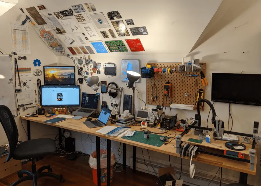
Engineer Workstation
The field of PCB design offers a diverse range of career paths, each with its own set of challenges and rewards. From working within established companies to forging a freelance career or specializing in niche industries, PCB designers have ample opportunities for professional growth and specialization.
In-House PCB Designer Many PCB designers work directly for companies that manufacture electronic products. This could range from large corporations to smaller tech startups. These roles typically provide a stable work environment, a structured career path, and opportunities to collaborate within a larger engineering team.
Freelance PCB Designer Freelancing offers flexibility and control over projects and schedules. Freelance designers typically manage their own business, client relationships, and project delivery. It can be a rewarding path for those who are self-motivated and comfortable with the entrepreneurial aspects of the job.
Specialized Industry PCB Designer Certain industries have specific demands and requirements for PCB designs. Specializations could include working in the aerospace, automotive, medical devices, or telecommunications sectors. These roles often require additional expertise in the standards and regulations specific to those fields.
PCB Design Consultant As consultants, PCB designers provide expert advice and solutions to various clients across different industries. They are hired for their specific skills to solve complex PCB design challenges and offer guidance on best practices.
PCB Design Team Lead/Manager Experienced PCB designers can advance to leadership roles where they manage and mentor teams of designers, overseeing projects and ensuring quality standards are met within a design department.
Career Path
Pros
Cons
In-House PCB Designer
Stable income, structured environment, team collaboration
Less flexibility, slower career progression, limited project diversity
Income instability, self-management required, finding clients
Specialized Industry PCB Designer
High demand, industry-specific challenges, competitive salary
May require extra qualifications, limited transferability to other industries
PCB Design Consultant
Diverse projects, higher earning potential, problem solving
Requires strong communication and client management skills, travel may be needed
PCB Design Team Lead/Manager
Leadership roles, mentoring, strategic planning
Management responsibility, less hands-on design work, high stress levels
Becoming a PCB Designer: Education, Certifications, and Training
PCB Training
Aspiring PCB designers can enter the field through various educational paths, certifications, and training programs. A strong foundation in electrical engineering principles is crucial, and while a formal degree isn't always mandatory, specialized training and certifications can significantly enhance career prospects. This section provides a practical guide on how to begin a journey as a PCB designer.
Formal Education A bachelor's degree in Electrical Engineering, Electronics Engineering, or a related field is beneficial, providing a strong theoretical understanding of circuit analysis, electromagnetism, and signal integrity. Some community colleges offer associate degrees or diplomas in electronics technology, which can be a quicker route to entry-level positions.
Specialized Training Programs Many vocational schools, technical institutes, and online platforms offer dedicated PCB design courses and programs. These programs typically focus on practical skills, including using industry-standard EDA software and applying design principles. These programs can be beneficial even with an engineering degree, offering hands-on training.
Industry Certifications Certifications, such as those offered by IPC (Association Connecting Electronics Industries), validate a designer's proficiency in specific areas like PCB design, assembly, and rework. The IPC CID (Certified Interconnect Designer) and CID+ (Certified Interconnect Designer Advanced) certifications are highly regarded in the industry. These certifications require passing exams that assess your knowledge and experience.
Software Proficiency Proficiency with CAD software such as Altium Designer, KiCad, Eagle, and OrCAD is indispensable. Consider focusing on one or two software suites to gain mastery, as these tools are essential for PCB design. There are many online tutorials, courses and bootcamps to help you learn the software and also to improve your knowledge.
Practical Experience Gaining hands-on experience through internships, personal projects, or entry-level positions is essential. Building a portfolio that showcases your design skills and the complexity of your work is extremely important to your professional development.
Freelancing as a PCB Designer
Remote PCB Designer
Freelancing offers PCB designers the flexibility to manage their own projects, set their own schedules, and work with diverse clients, but it also requires a strong business acumen and self-discipline to manage the inherent challenges of client acquisition and project management.
Pros of Freelancing Flexibility in work hours and location, potential for higher earnings, diverse project portfolio, and the autonomy to choose projects aligned with personal interests and expertise.
Cons of Freelancing Inconsistent income, responsibility for self-marketing and client acquisition, managing finances, taxes, and administrative tasks, and the need for robust self-discipline.
To succeed as a freelance PCB designer, consider these key areas:
Finding Clients Utilize online platforms such as Upwork, Fiverr, and LinkedIn, network through industry events, and leverage referrals from previous clients and colleagues.
Project Management Clearly define project scopes, set realistic deadlines, maintain open communication with clients, and use project management tools to track progress and ensure timely delivery.
Building a Successful Business Create a professional portfolio showcasing past work, develop a strong brand identity, set competitive pricing, manage finances effectively, and continually invest in skill development.
Freelancing as a PCB designer can be a rewarding career path for those who are self-motivated and possess strong technical skills. With a well-structured approach to client acquisition, project management, and business development, freelance PCB designers can achieve both professional and financial success.
Frequently Asked Questions About PCB Designers
This section addresses common questions regarding PCB designers, covering their roles, costs, demand, and paths to entering the field. It aims to provide clear, concise answers to help anyone understand the profession better.
What exactly does a PCB designer do? PCB designers translate electronic schematics into physical layouts of printed circuit boards. This includes component placement, trace routing, ensuring signal integrity, and considering thermal management and manufacturability.
How much does it cost to hire a PCB designer? The cost to hire a PCB designer varies widely depending on experience, complexity of the design, and project scope. Rates can range from hourly fees for freelancers to fixed project costs. Factors like the number of layers, component density, and required precision also impact the cost.
Is there high demand for PCB designers? Yes, the demand for skilled PCB designers remains consistently high. With the increasing complexity of electronic devices and the growth of industries such as consumer electronics, automotive, and aerospace, there is a continuous need for competent PCB design professionals.
How many PCB designers are working in the field? While precise global figures are difficult to obtain, the number of PCB designers is substantial, reflecting the ubiquity of electronics in modern society. The field is sufficiently large to support diverse specializations and career paths, yet small enough to warrant that skilled individuals will have ample opportunities.
What education and training are needed to become a PCB designer? A formal education in electrical engineering or a related field can be beneficial, but not always mandatory. Essential skills are often gained through technical schools, online courses, and practical experience. Knowledge of EDA software like Altium Designer, KiCad, or Eagle, and a grasp of fundamental electronics, are highly valued. IPC certifications can also enhance job prospects.
What are the typical challenges faced by PCB designers? Common challenges include managing signal integrity, minimizing electromagnetic interference (EMI), ensuring thermal management, optimizing designs for manufacturability, and keeping up with the latest technological advancements. Designers also face time constraints and balancing competing design priorities.
Can PCB design be done remotely? Yes, many PCB designers work remotely, leveraging cloud-based design tools and collaboration platforms. This flexibility is beneficial for both freelancers and employees, allowing access to talent across geographical boundaries.
Future Trends in PCB Design
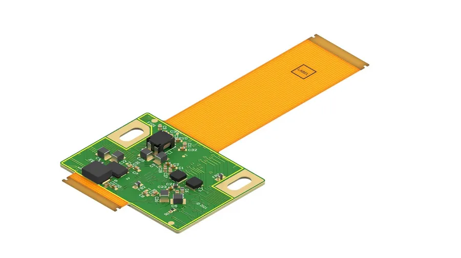
Flexible PCB
The field of PCB design is rapidly evolving, driven by advancements in technology and the increasing complexity of electronic devices. Understanding these future trends is crucial for PCB designers to stay competitive and innovative. This section explores key emerging areas that are shaping the future of PCB design.
High-Density Interconnect (HDI) PCBs HDI PCBs are becoming increasingly important for smaller and more complex devices. These boards feature microvias, finer lines, and smaller spacing, enabling higher component density and improved electrical performance. The trend is towards further miniaturization and increased functionality in devices, pushing HDI technology to the forefront.
Advanced Materials The demand for enhanced thermal management, improved signal integrity, and reduced signal loss is driving research into advanced PCB materials. We're seeing increasing use of materials with lower dielectric constants, better thermal conductivity, and enhanced mechanical properties to meet the stringent requirements of modern electronics. Examples include composite materials and nanomaterials.
Flexible and Stretchable PCBs Flexible PCBs are revolutionizing wearable tech, medical devices, and automotive applications. These boards can conform to complex shapes and withstand bending or flexing. Stretchable PCBs take this further, allowing for even more dynamic applications. Future developments will emphasize improved reliability and durability of these flexible and stretchable boards.
3D Printing of PCBs Additive manufacturing, or 3D printing, is transforming PCB prototyping and low-volume production. This technique enables rapid iterations, complex designs, and the potential for customized boards. While still relatively nascent, advancements in materials and printing technology point toward wider adoption in the near future.
AI and Machine Learning in PCB Design Artificial intelligence (AI) and machine learning (ML) are making their way into PCB design tools. These technologies can automate routine tasks, optimize layouts, and predict design issues, greatly enhancing efficiency and accuracy. Expect to see increased integration of AI and ML in EDA software for more intelligent and automated PCB design workflows.
Increased Focus on Sustainability Environmental concerns are increasingly influencing PCB design. Designers are exploring more sustainable materials, eco-friendly manufacturing processes, and strategies for recycling electronic waste. The focus will continue to shift towards minimizing the environmental footprint of PCB production and disposal.
The role of PCB designers is critical to the technological advancements we see every day. From smartphones to spacecraft, PCB designers are behind the innovative electronics that drive our world. This article has provided insights into the multifaceted responsibilities, essential skills, and various career pathways within the field. For PCB designers, both experienced and aspiring, it’s essential to embrace continuous learning and stay updated on the latest trends and technologies. The future of electronics is closely tied to the expertise of skilled PCB designers, making it a field with a bright and impactful future.