The printed circuit board (PCB) is the unsung hero of modern electronics, the foundation upon which our digital world is built. From smartphones to spacecraft, PCBs are essential. This article demystifies the intricate process of PCB production, detailing each critical step and ensuring a comprehensive understanding of how these essential components are brought to life. We'll journey from the initial design phase to the final, functional circuit board, uncovering the technology and expertise that go into every manufactured PCB.
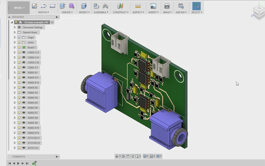
The genesis of any printed circuit board (PCB) lies in its meticulous design and layout phase. This foundational step employs Computer-Aided Design (CAD) software to translate electrical requirements into a physical blueprint, defining component placement, electrical pathways, and overall board functionality. Accurate design at this stage is paramount, as it directly impacts signal integrity, thermal management, and the manufacturability of the final product.
| Aspect | Description | Importance |
|---|---|---|
| Schematic Capture | Creation of the electrical circuit diagram representing the interconnection of components. | Defines the functional requirements of the PCB. |
| PCB Layout | Physical arrangement of components, traces, and other elements on the board. | Ensures electrical functionality, signal integrity and facilitates manufacturability. |
| CAD Software | Specialized software tools (e.g., Altium Designer, Eagle, KiCad) used for schematic capture and PCB layout. | Enables precise and efficient PCB design. |
| Signal Integrity | Ensuring the quality and fidelity of electrical signals as they propagate through traces. | Crucial for high-speed and analog circuits. |
| Thermal Management | Designing the board to dissipate heat effectively, preventing component overheating. | Ensures reliability and performance of the PCB. |
| Manufacturability | Designing the PCB with consideration for the capabilities of the manufacturing processes and equipment. | Reduces manufacturing costs and improves yield. |
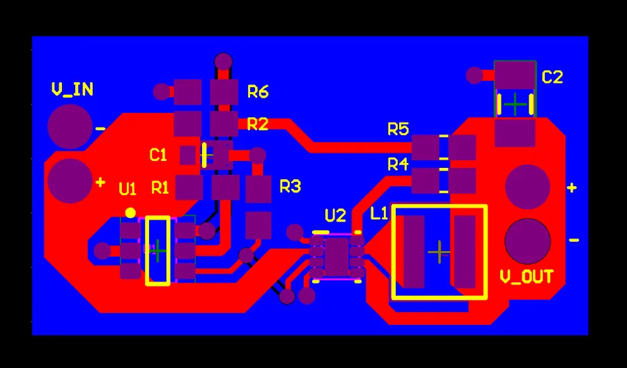
The transition from a completed PCB design to its physical manufacturing hinges on the accurate generation of Gerber files. These files serve as the standardized digital blueprint, conveying every critical detail of the PCB layout to the fabrication equipment. A comprehensive set of Gerber files is essential for a seamless and precise manufacturing process, dictating the precise copper layers, solder mask, silkscreen, and drill hole locations.
| Gerber File Extension | Description | Purpose |
|---|---|---|
| .GTL | Top Copper Layer | Defines the top layer copper traces and pads |
| .GBL | Bottom Copper Layer | Defines the bottom layer copper traces and pads |
| .GTS | Top Solder Mask | Defines the top solder mask layer |
| .GBS | Bottom Solder Mask | Defines the bottom solder mask layer |
| .GTO | Top Silkscreen Layer | Defines the top silkscreen layer |
| .GBO | Bottom Silkscreen Layer | Defines the bottom silkscreen layer |
| .TXT | Drill File | Defines drill hole locations and sizes |
| .GKO | Keepout Layer | Defines areas where components cannot be placed |
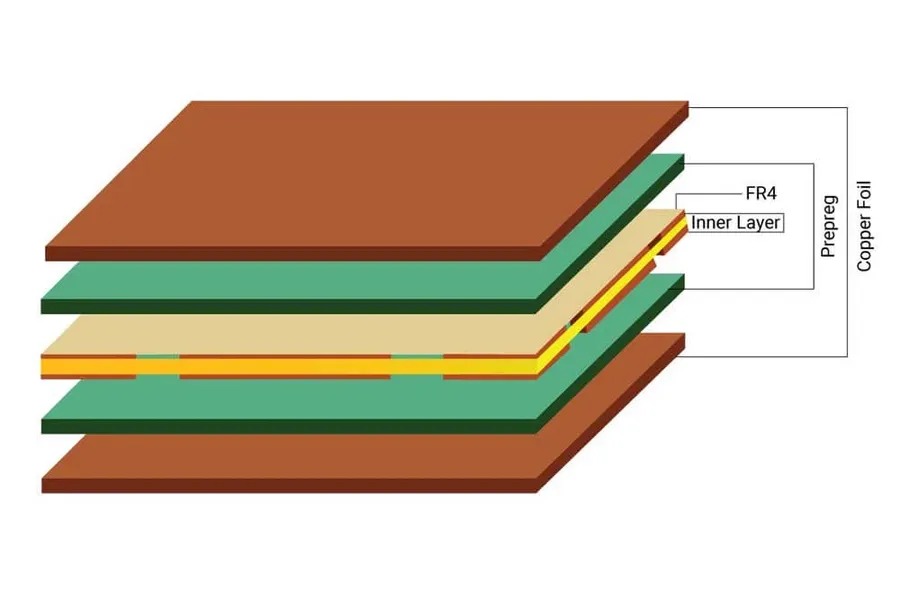
The selection of appropriate materials is paramount in PCB production, as it directly influences the final performance and reliability of the board. This decision hinges on a careful evaluation of the intended application, operating environment, and performance requirements, affecting both the mechanical and electrical characteristics of the finished PCB.
| Material | Description | Typical Applications | Advantages | Disadvantages |
|---|---|---|---|---|
| FR-4 | A composite material made of woven fiberglass cloth with epoxy resin. | General-purpose PCBs, most consumer electronics. | Cost-effective, good mechanical strength, widely available. | Limited thermal performance, not suitable for high-frequency applications. |
| High-Tg FR-4 | FR-4 with higher glass transition temperature. | Higher-temperature applications, automotive electronics. | Improved thermal resistance compared to standard FR-4. | More expensive than standard FR-4. |
| Polyimide | A high-performance polymer. | Aerospace, high-temperature, and flexible circuits. | Excellent thermal stability, good electrical properties, flexible. | More expensive, may be sensitive to moisture absorption. |
| PTFE (Teflon) | A fluoropolymer. | High-frequency applications, microwave circuits, RF applications. | Excellent electrical performance, low dielectric constant, low loss. | Expensive, can be difficult to process. |
| Metal Core (Aluminum, Copper) | A metal base with a dielectric layer. | High-power electronics, LED lighting, thermal management. | Excellent thermal conductivity, good heat dissipation. | Can be heavier and more costly |
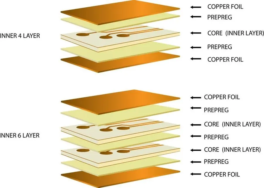
In the production of multi-layer PCBs, the fabrication of inner layers is a critical early step. This process involves transferring the designed circuit patterns onto copper-clad laminates, followed by precise etching to remove excess copper, thereby forming the conductive traces. This stage demands high precision and control to ensure dimensional accuracy of the internal circuitry.
| Process Step | Description | Key Considerations |
|---|---|---|
| Preparation | Cleaning and preparing the copper-clad laminate for photoresist application. | Ensuring a clean, contaminant-free surface for optimal adhesion. |
| Photoresist Application | Applying a photosensitive material onto the copper surface. | Uniform coating thickness and minimal defects. |
| Exposure | Exposing the photoresist to UV light through a mask containing the circuit pattern. | Accurate alignment of the mask to the copper layer, sufficient UV intensity for proper curing. |
| Development | Removing unexposed photoresist using a chemical solution. | Proper chemical concentration and temperature for complete removal of unwanted photoresist. |
| Etching | Chemically removing the unprotected copper to form the circuit traces. | Precise control of etching parameters (time, temperature, chemical concentration) to achieve desired trace width and shape. |
| Photoresist Removal | Removing the remaining photoresist after etching. | Complete removal of the photoresist to prepare for the next process. |
| Inspection | Verifying the quality of the etched traces against design specifications. | Ensuring the dimensional accuracy and integrity of the circuit patterns. |
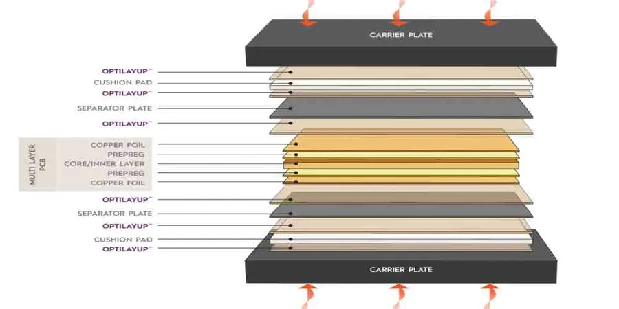
Lamination and layer bonding are critical processes in multi-layer PCB production, where pre-fabricated inner layers are meticulously stacked and fused to form the core structure of the printed circuit board. This step involves the application of controlled heat and pressure to ensure a homogenous bond, creating a robust, multi-layered substrate for further processing.
Key aspects of this process include:
| Parameter | Description | Impact on PCB |
|---|---|---|
| Lamination Temperature | Temperature at which heat is applied during bonding | Affects resin melting, bonding strength, and laminate properties |
| Lamination Pressure | Force applied during the bonding process | Ensures proper resin flow, good contact, and layer bonding |
| Curing Time | Duration of heat and pressure during lamination | Impacts resin curing and the dimensional stability of the PCB |
| Prepreg Material | Type of bonding agent used between layers | Determines dielectric properties, layer adhesion, and thermal resistance |
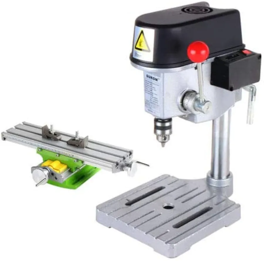
The drilling and plating stage in PCB production is critical for establishing electrical connections between different layers of a multi-layer board and for creating mounting points for components. This process involves creating precise holes through the laminated PCB stack-up, followed by plating the interior of these holes with copper.
This ensures the functionality of a multi-layer PCB by enabling the interconnections between layers.
| Parameter | Description | Typical Value |
|---|---|---|
| Drill Bit Diameter | Size of the drill bit used to create vias and component holes. | 0.1 mm - 1.0 mm |
| Copper Plating Thickness | Thickness of copper deposited within drilled holes. | 20 - 30 µm |
| Hole Positional Accuracy | Accuracy of drill hole location relative to design. | ± 0.05 mm |
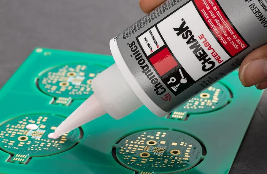
The application of solder mask and silkscreen printing are critical steps in PCB production, serving distinct yet complementary purposes. The solder mask acts as a protective layer, preventing unintended solder connections, while the silkscreen provides crucial labeling for component placement and identification, ensuring efficient assembly and maintenance of the board.
| Feature | Solder Mask | Silkscreen |
|---|---|---|
| Primary Function | Prevents Solder Bridges; Protects Traces | Provides Component Labels & Markings |
| Material | Epoxy or Polymer | Specialized Ink |
| Application Method | Screen Printing/Photolithography | Screen Printing |
| Position | Applied over copper traces | Applied over solder mask |
| Color | Usually Green; Other Colors Available | Usually White or Yellow |
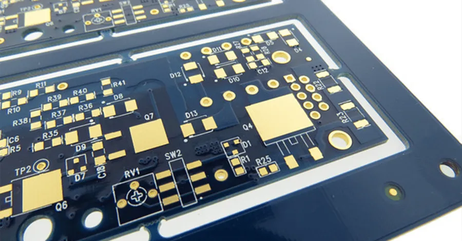
The application of a surface finish to the exposed copper pads on a PCB is a critical step in the manufacturing process, serving to enhance both solderability and protection against corrosion. This ensures reliable electrical connections and prolongs the lifespan of the board. The selection of the appropriate surface finish is often dictated by the specific requirements of the application, including factors such as cost, environmental conditions, and desired performance characteristics.
| Surface Finish Type | Description | Advantages | Disadvantages |
|---|---|---|---|
| HASL (Hot Air Solder Leveling) | A coating of molten solder applied to the copper pads and then leveled with hot air. | Low cost, good solderability, robust. | Uneven surface, not ideal for fine-pitch components, contains lead (in leaded HASL). |
| ENIG (Electroless Nickel Immersion Gold) | A layer of nickel is deposited on the copper followed by a thin layer of gold. | Excellent solderability, good for wire bonding, flat surface. | Higher cost, potential for 'black pad' issues. |
| Immersion Tin | A thin layer of tin is chemically deposited on the copper. | Good solderability, lead-free, relatively low cost. | Susceptible to tin whiskers, short shelf life. |
| Immersion Silver | A thin layer of silver is chemically deposited on the copper. | Good solderability, lead-free, good for fine-pitch components. | Susceptible to tarnishing, migration issues under high humidity. |
| OSP (Organic Solderability Preservative) | A thin, water-based organic coating that protects the copper from oxidation. | Low cost, good solderability, lead-free. | Very short shelf life, easily damaged during handling, not suitable for multiple reflow cycles. |
Rigorous electrical testing and quality control are crucial steps in PCB production, ensuring that fabricated boards meet the required specifications and perform as intended before component assembly. These procedures identify potential defects early, preventing costly rework and ensuring the reliability of the final product.
The testing phase typically involves a combination of automated and manual methods to verify circuit integrity, impedance characteristics, and overall functionality. These tests are designed to detect manufacturing flaws such as shorts, opens, and incorrect component connections, all of which can compromise the functionality of the board.
Quality control measures are implemented to maintain consistent manufacturing standards and identify areas for process improvements. Data collected during testing provides valuable insights for optimizing production and enhancing the overall reliability of the final product.
| Test Type | Description | Purpose |
|---|---|---|
| Continuity Test | Checks for open circuits in traces and vias. | Ensures proper electrical connections. |
| Short Circuit Test | Identifies unintended connections between different parts of the circuit. | Prevents malfunctions due to shorts. |
| Impedance Test | Verifies that the impedance of traces falls within the specified tolerance. | Maintains signal integrity. |
| Flying Probe Test | Automated test using probes to check electrical connections without a dedicated test fixture. | Flexible testing for prototypes and low volume runs |
| Bed-of-Nails Test | Utilizes a fixture with multiple spring-loaded pins to test multiple points on the board simultaneously. | Fast high-volume testing. |
This section addresses common queries regarding PCB (Printed Circuit Board) production, providing concise and informative answers based on engineering principles and industry best practices.
PCB production is a sophisticated process combining design expertise with advanced manufacturing techniques. Each stage, from initial design to final testing, plays a crucial role in ensuring the quality and reliability of the finished product. Understanding this intricate process is essential for anyone involved in electronics engineering and design, as it enables the creation of increasingly complex and efficient electronic devices. By staying informed about advancements in PCB production technology, we can continue to push the boundaries of what is possible in the digital age. From simple single-layer boards to highly complex multi-layer PCBs, the future of electronics is closely intertwined with progress in PCB manufacturing.

