From the smartphone in your hand to the power grid that lights up your city, MOSFETs and their inherent capacitance are fundamental to modern electronics. This article delves into the often overlooked, yet critical role of MOSFET capacitors in circuit design. We'll explore how these tiny components influence everything from switching speed to signal integrity, bridging the gap between theoretical concepts and their practical applications in our technology-driven world. Prepare to uncover the mysteries of the MOSFET capacitor.
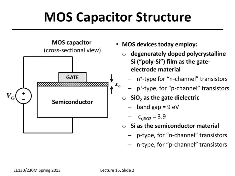
The Metal-Oxide-Semiconductor (MOS) capacitor serves as the foundational element for MOSFETs, embodying a layered structure designed to store electrical charge. This fundamental component is critical to understanding the behavior of MOSFETs and their applications in modern electronics.
A MOS capacitor consists of three primary layers: a metallic gate electrode, an insulating oxide layer (typically silicon dioxide), and a semiconductor substrate. The application of a voltage across these layers allows for the accumulation or depletion of charge carriers in the semiconductor material, giving rise to capacitance.
| Layer | Material | Function |
|---|---|---|
| Metal Gate | Aluminum, Polysilicon, or other conductive material | Acts as one capacitor plate; voltage application point |
| Oxide Layer | Silicon Dioxide (SiO2) or high-k dielectric | Insulator preventing current flow between gate and semiconductor |
| Semiconductor Substrate | Silicon (Si), typically doped | Forms the other capacitor plate; charge accumulation occurs here |
The key to charge storage in a MOS capacitor lies in the modulation of charge carriers (electrons or holes) within the semiconductor substrate, induced by the applied gate voltage. This forms a depletion region or an inversion layer depending on the applied voltage polarity, resulting in capacitance changes and underlying the basic functionality of the MOS capacitor.
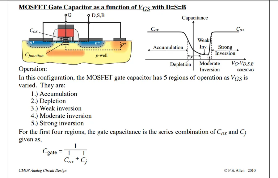
MOSFET gate capacitance (Cgs), primarily formed by the gate-source overlap and the gate channel region, is a critical parameter influencing both the switching speed and power consumption of a MOSFET. Understanding this capacitance is fundamental to effective circuit design. This section will delve into the nature of Cgs, its impact on circuit performance, and how to effectively interpret datasheet specifications.
| Parameter | Description | Impact |
|---|---|---|
| Gate-Source Capacitance (Cgs) | Capacitance between the gate and source terminals. | Influences switching speed, input impedance, and power consumption. |
| Gate-Drain Capacitance (Cgd) | Capacitance between the gate and drain terminals. | Contributes to the Miller effect, affecting high-frequency response and stability. |
| Gate-Bulk Capacitance (Cgb) | Capacitance between the gate and bulk terminals. | Usually less significant than Cgs or Cgd, but may affect the device characteristics. |
The gate capacitance (Cgs) arises from the physical structure of the MOSFET, where the gate electrode, separated by a thin oxide layer from the channel, behaves as a capacitor. The accumulation of charge on both sides of this dielectric forms the gate capacitance. This capacitance presents an impedance to the driving signal, affecting the rate at which the MOSFET can switch between its on and off states. A higher Cgs typically results in slower switching speeds and increased power losses during switching transitions due to the energy required to charge and discharge this capacitance.
Datasheets for MOSFETs typically provide a value for input capacitance (Ciss), which is effectively the sum of Cgs and Cgd, and a value for Cgs. When analyzing MOSFET characteristics for circuit design, these capacitance values are used to model the device behavior. Understanding how these capacitance values vary with operating conditions, such as voltage or temperature, is crucial in achieving predictable and efficient circuit designs. Moreover, the datasheets often include graphs and charts illustrating these variations, further aiding in the selection and implementation process.
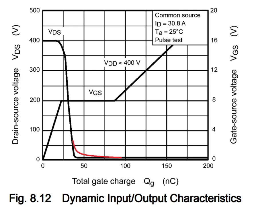
The Miller effect is a phenomenon where the effective gate-drain capacitance (Cgd) of a MOSFET appears amplified when viewed from the input side (gate), significantly impacting high-frequency circuit performance. This amplification arises due to the feedback path through Cgd, influencing both gain and bandwidth, and necessitating careful consideration in circuit design.
Specifically, the Miller effect effectively increases the input capacitance, which is crucial to understand when driving a MOSFET. This effect is not just a theoretical concern, it manifests in real-world circuits, causing delays, bandwidth limitations, and instability if not properly addressed.
| Parameter | Description | Impact |
|---|---|---|
| Miller Capacitance | Effective increase in gate capacitance due to Cgd feedback | Reduces bandwidth, increases switching delays |
| Amplification Factor | Gain dependent amplification of Cgd | Distorts frequency response, can cause oscillations |
| Gate-Drain Capacitance (Cgd) | Physical capacitance between gate and drain terminals | Primary contributor to Miller effect |
| Load Impedance | Output impedance connected to the drain | Influences the degree of Miller effect |
Mitigating the Miller effect is crucial for optimizing circuit performance. Several techniques can be applied to minimize its impact. Selecting appropriate MOSFETs with low Cgd values can significantly reduce the initial Miller capacitance.
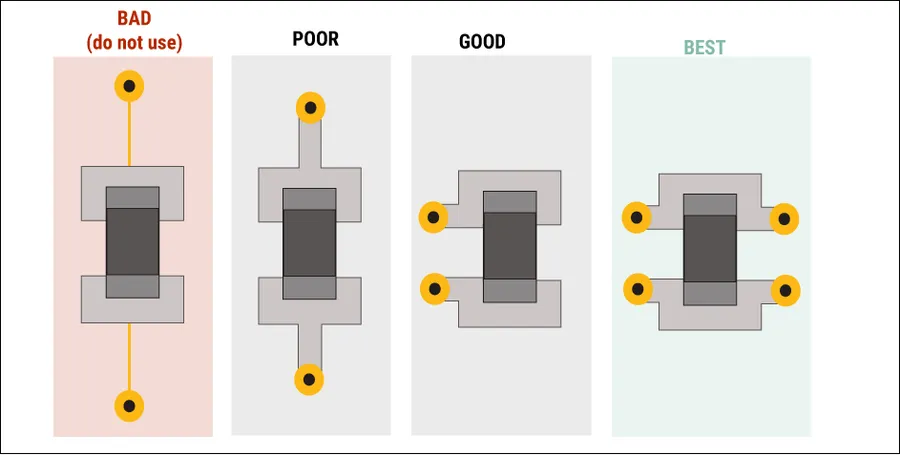
Decoupling capacitors are essential components in MOSFET circuits, serving as local energy reservoirs to ensure a stable power supply and mitigate noise. By providing a low-impedance path for high-frequency current fluctuations, they prevent voltage drops and signal degradation that can compromise the performance of the MOSFET and associated circuitry. These capacitors are typically placed physically close to the MOSFET, minimizing parasitic inductance and maximizing their effectiveness.
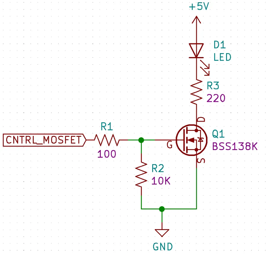
External capacitors play a crucial role in shaping the behavior of MOSFET circuits, going beyond the inherent parasitic capacitances within the device itself. These external components are strategically added to achieve specific circuit functionalities, such as filtering, energy storage, and impedance matching. This section delves into the common applications of these capacitors, focusing on gate-source and source-drain configurations, and their impacts on circuit performance.
When connecting external capacitors to MOSFET circuits, careful selection of capacitor type, capacitance value, and voltage rating is crucial, along with consideration of parasitic inductance from capacitor leads or mounting pads, ensuring optimal circuit performance.
| Application | Capacitor Placement | Impact on MOSFET Operation |
|---|---|---|
| Gate Switching Speed Control | Gate to Source (Cgs) | Reduces switching speed; filter noise |
| Snubber Circuit | Source to Drain (Cds) | Suppresses voltage transients, limits EMI |
| High-Side Gate Driver | Gate and a voltage source | Provides a temporary voltage source |
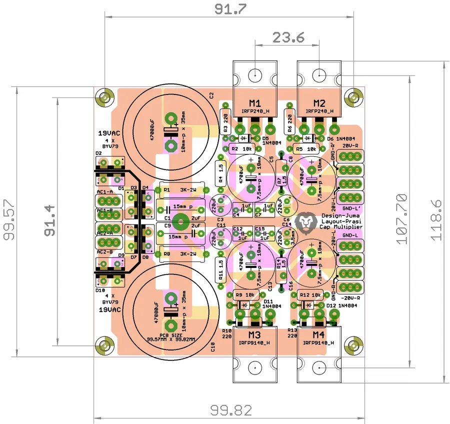
MOSFETs can be ingeniously employed in capacitor multiplier circuits to achieve effective capacitance values significantly greater than those of the physical capacitors used. This technique is pivotal in applications where large capacitance is required but physical space or component availability limits the use of large discrete capacitors. These circuits cleverly leverage the transconductance of the MOSFET to amplify the apparent capacitance.
These circuits are particularly useful in various applications, such as: low-frequency filtering, power supply smoothing, and analog circuit compensation. The ability to achieve high equivalent capacitances without using physically large capacitors offers significant advantages in terms of space savings, cost reduction, and improved circuit integration.
The basic principle involves using a MOSFET as an active device within a feedback loop. By carefully configuring the feedback and biasing, the circuit can simulate the behavior of a large capacitor even though a much smaller physical capacitor is employed. The Miller effect, previously discussed in relation to parasitic capacitance, is intentionally harnessed to amplify the effective capacitance seen by the circuit.
Key aspects of MOSFET-based capacitor multipliers include the selection of appropriate MOSFET parameters, such as transconductance and gate capacitance, to achieve the desired effective capacitance and bandwidth. Furthermore, the design must carefully consider stability and noise performance to ensure reliable and accurate circuit operation. It's important to note that practical limitations do exist. The effective capacitance and frequency response will be limited by factors including MOSFET transconductance and parasitic capacitance.
Let's consider a basic implementation. In a common configuration, the MOSFET operates in its active region, and the physical capacitor is placed in the feedback path. The effective capacitance, Ceff, can be approximated by: Ceff ≈ (1 + gm * R) * C, where 'gm' represents the MOSFET's transconductance, 'R' is the resistance in the feedback loop, and 'C' is the physical capacitance. This equation demonstrates how the MOSFET's transconductance acts as a multiplier to increase the effective capacitance.
| Parameter | Description |
|---|---|
| MOSFET Transconductance (gm) | Determines the amplification factor of the capacitor multiplier. |
| Feedback Resistance (R) | Along with gm, influences the effective capacitance. |
| Physical Capacitance (C) | The actual capacitor value used in the circuit. |
| Effective Capacitance (Ceff) | The apparent capacitance as a result of the multiplier. |
This section addresses common questions about MOSFET capacitors, clarifying their role, functionality, and differences from related components. It aims to provide clear and concise answers to the most frequently asked questions regarding MOSFET capacitors and their applications in circuit design.
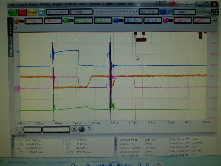
MOSFET capacitance is a critical factor that directly influences the switching speed of circuits. The inherent capacitances within a MOSFET, particularly gate-source capacitance (Cgs) and gate-drain capacitance (Cgd), limit how quickly the device can transition between its ON and OFF states. Understanding this relationship is crucial for optimizing circuit performance, particularly in high-speed applications.
| Capacitance Type | Symbol | Impact on Switching Speed | Description |
|---|---|---|---|
| Gate-Source Capacitance | Cgs | Increased Cgs slows down charging of the gate | Capacitance between the gate and source terminals, influencing the charge required to turn on the MOSFET. |
| Gate-Drain Capacitance | Cgd | Amplified by the Miller effect, leading to switching delays | Capacitance between the gate and drain terminals, contributing to the Miller effect. |
| Drain-Source Capacitance | Cds | Can affect signal integrity and introduce parasitic effects | Capacitance between the drain and source terminals, typically smaller but still relevant. |
The primary limitation on switching speed arises from the time required to charge and discharge these capacitances. Higher capacitance values necessitate more charge transfer, which consequently slows down the switching transitions. Moreover, the Miller effect, driven by Cgd, further compounds the issue by effectively multiplying the gate capacitance, making the charge-discharge process more time-consuming.
Achieving faster switching speeds requires careful design considerations aimed at minimizing the impact of MOSFET capacitances. Techniques include: utilizing MOSFETs with lower intrinsic capacitances, optimizing driver circuits to supply sufficient current for fast charging and discharging, and employing circuit topologies that minimize the Miller effect. These considerations are essential for high-speed applications where timing and efficiency are crucial.
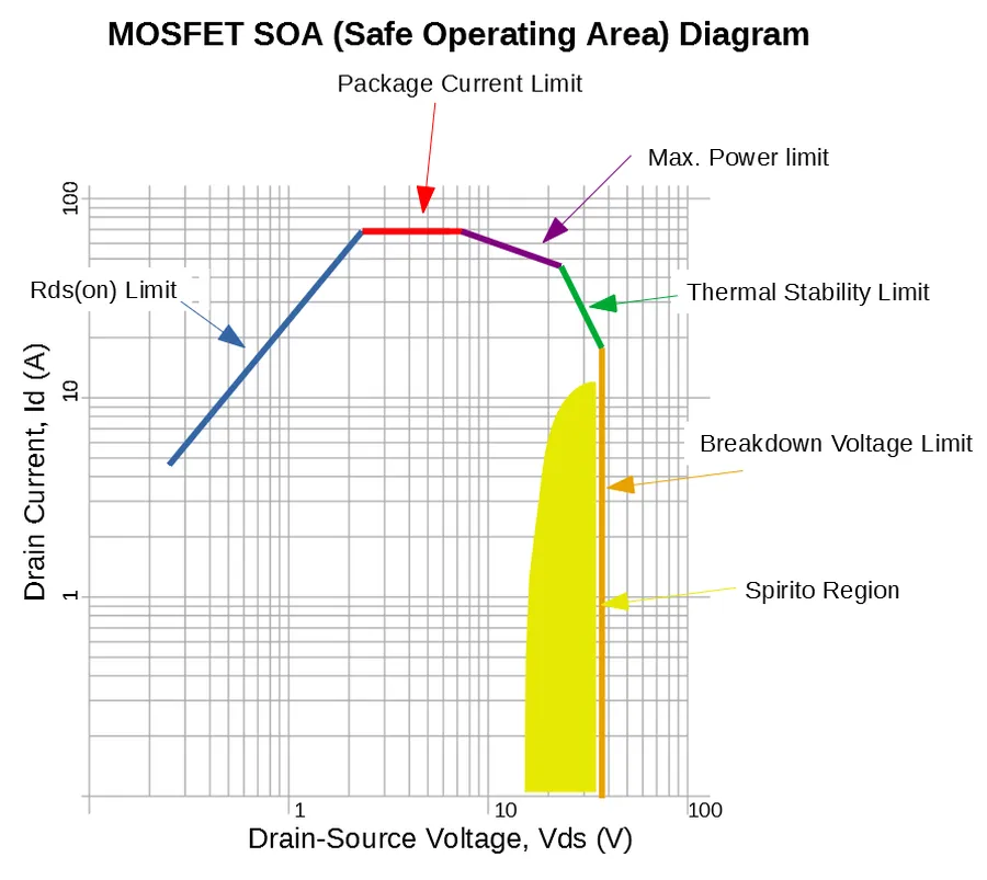
MOSFET capacitance is not a fixed value; it varies significantly due to process variations during manufacturing. These variations lead to different performance characteristics, which are often categorized into technology corners such as Fast-Fast (FF), Slow-Slow (SS), Fast-Slow (FS), and Slow-Fast (SF). Understanding these corners is crucial for robust circuit design.
| Technology Corner | Description | Impact on Capacitance | Impact on Switching Speed |
|---|---|---|---|
| Fast-Fast (FF) | Both NMOS and PMOS transistors are faster than nominal. | Lower capacitance values. | Faster switching speed, potentially higher power consumption. |
| Slow-Slow (SS) | Both NMOS and PMOS transistors are slower than nominal. | Higher capacitance values. | Slower switching speed, potentially lower power consumption. |
| Fast-Slow (FS) | NMOS transistor is faster, PMOS is slower. | NMOS capacitance lower, PMOS capacitance higher. | Asymmetric switching characteristics. |
| Slow-Fast (SF) | NMOS transistor is slower, PMOS is faster. | NMOS capacitance higher, PMOS capacitance lower. | Asymmetric switching characteristics. |
These variations in capacitance directly affect circuit performance. For instance, the FF corner, with its lower capacitance, often results in faster switching speeds but also increased power consumption. Conversely, the SS corner tends to have slower switching but lower power consumption. Designers must account for these variations to ensure that the circuit functions reliably across all operating corners.
In conclusion, MOSFET capacitors, though seemingly small components, have a significant impact on the performance of electronic circuits. Understanding gate capacitance, the Miller effect, and the use of decoupling capacitors and capacitor multiplier is essential for every electronic engineer to optimize circuit performance and reliability. By correctly analyzing and leveraging the properties of MOSFET capacitors, we can design increasingly efficient and powerful technologies that drive progress in every field. The future of electronics is inevitably tied to continued innovation in MOSFET and capacitor technology.

