Imagine a tiny electronic wizard using switches to precisely control the flow of energy in a circuit – that's the essence of a switched capacitor. These ingenious circuits, unlike their traditional counterparts, utilize capacitors and electronic switches to mimic the behavior of resistors, opening up a world of possibilities in microelectronics and beyond. In this article, we'll delve into the intricacies of switched capacitor circuits, uncovering their advantages, applications, and the magic they bring to modern technology.
Switched capacitor circuits leverage the dynamic transfer of charge between capacitors, controlled by switches, to emulate the behavior of resistors and other analog circuit elements. This approach, pivotal in modern integrated circuit design, allows for precise and tunable analog functions without relying on traditional, often bulky, resistive components. The core mechanism revolves around the periodic connection and disconnection of capacitors to different circuit nodes, effectively moving charge and thus mimicking resistance or other analog functionalities.
The operation of a switched capacitor circuit is based on two fundamental phases, typically controlled by a clock signal. During the first phase, a capacitor is charged to a specific voltage. In the subsequent phase, the capacitor is then connected to a different part of the circuit, transferring a portion of its stored charge. By rapidly switching between these phases, controlled by the clock frequency, a continuous flow of charge is created, acting as a current source that is proportional to the switching frequency and the capacitor value. This mechanism allows for the emulation of a resistance, the value of which can be precisely controlled by the ratio of two capacitors or the switching frequency, and is described by the equation R=1/(f*C), where f is the clock frequency, and C is the capacitance value. This approach allows for extremely precise and temperature stable 'resistors'.
Switched capacitor circuits offer an alternative to traditional resistors, particularly in integrated circuit (IC) design. By mimicking the behavior of resistors through controlled charge transfer between capacitors, they provide several advantages in terms of size, precision, and tunability, primarily determined by capacitor ratios.
| Feature | Traditional Resistor | Switched Capacitor 'Resistor' |
|---|---|---|
| Size | Relatively large, especially for high resistance values | Small footprint, ideal for on-chip integration |
| Precision | Limited by fabrication tolerances, can vary significantly | Highly precise, determined by capacitor ratios which are easier to control |
| Tunability | Fixed value, requires external adjustment or replacements | Easily tunable by adjusting the switching frequency and/or capacitor ratios |
| Temperature Sensitivity | Resistance value changes significantly with temperature | Less sensitive to temperature variations, but clock frequency can drift |
| Linearity | Generally linear (for ohmic resistors) | Can be non-linear, especially at high frequencies, requires proper design |
| Power Consumption | Dissipates power as heat | Lower power consumption, energy transfer between capacitors |
| Implementation | Requires dedicated fabrication steps | Easily implemented on-chip using standard CMOS process |
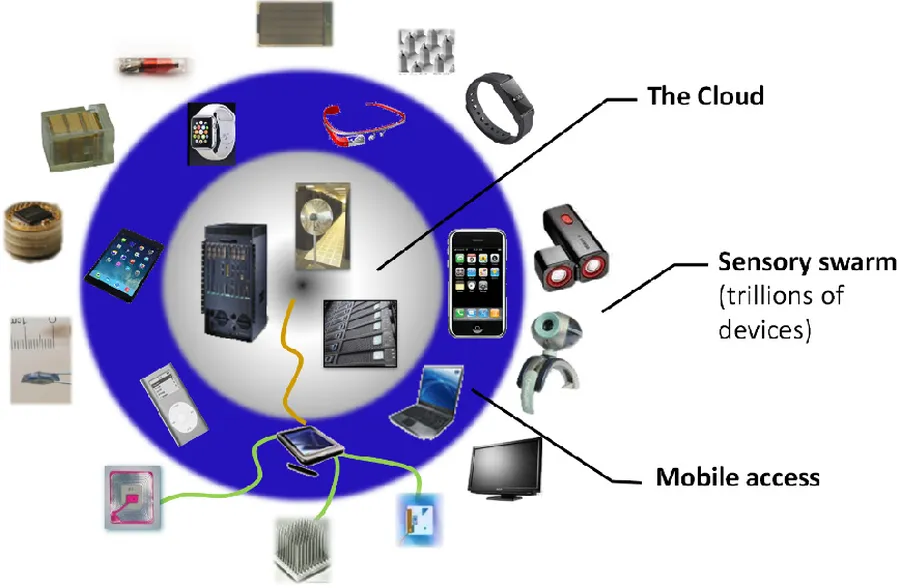
Switched capacitor circuits offer numerous benefits over traditional analog circuit design, particularly in integrated circuit (IC) implementations. These advantages stem from their ability to mimic resistor behavior using capacitors and switches, leading to more efficient and versatile designs.
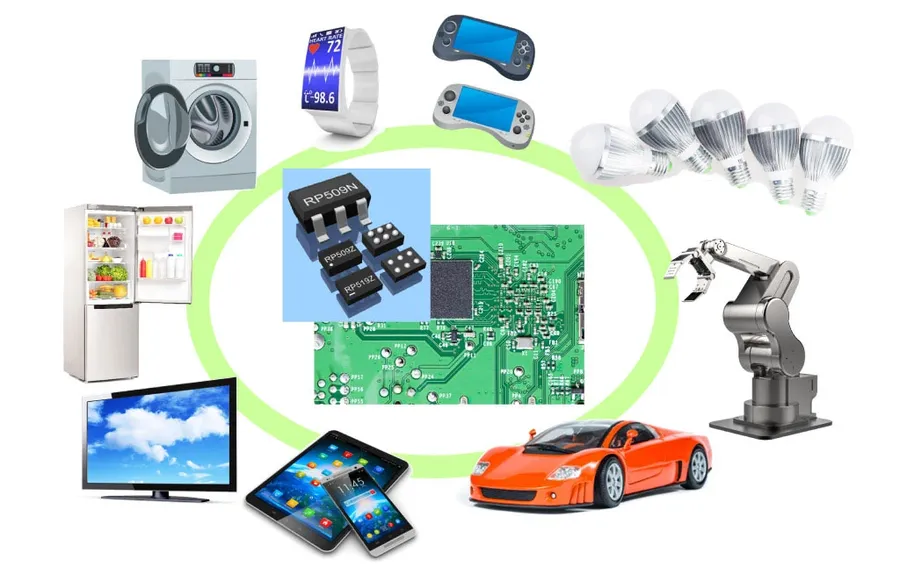
Switched capacitor circuits, owing to their versatility and ease of integration, find widespread use across various electronic applications. Their ability to mimic resistor behavior using capacitors and switches enables the creation of precise and tunable analog functions directly on integrated circuits (ICs).
Here's a detailed look into the primary application areas:
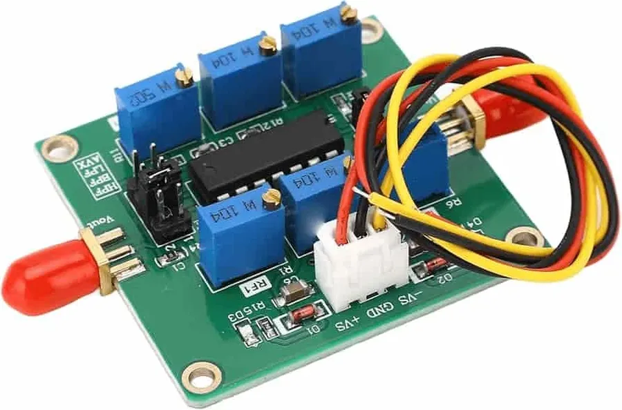
Switched capacitor (SC) circuits are ingeniously employed to realize filter functions, providing a compact and tunable alternative to traditional resistor-capacitor (RC) filters, particularly within integrated circuit (IC) designs. The fundamental principle involves using switches and capacitors to simulate the behavior of resistors, allowing for the creation of precise and adjustable filtering characteristics.
The operation of an SC filter revolves around the precise timing of switches that control the charging and discharging of capacitors. By alternating the connection of these capacitors, charge is transferred, mimicking the behavior of current flow through a resistor. The effective resistance is determined by the switching frequency and the capacitor value, providing a mechanism to implement different filter types. The key to filter design lies in choosing the appropriate topology and capacitor ratios to achieve the desired frequency response.
SC filters offer several advantages, especially in IC implementation. They do not require large resistors, which are difficult to integrate onto silicon. The precision of these filters is determined by capacitor ratios, which are controlled very accurately during manufacturing. Additionally, the filter characteristics can be tuned by adjusting the clock frequency, providing flexibility and programmability. The sampling frequency, directly related to the clock frequency, plays a critical role in determining the performance of the filter, with the Nyquist theorem as a significant factor in understanding potential aliasing issues.
| Filter Type | Frequency Response | Typical Application | Switched Capacitor Implementation Notes |
|---|---|---|---|
| Low-Pass Filter | Passes low frequencies and attenuates high frequencies | Anti-aliasing filters, audio processing | Effective capacitance at the output creates a low pass characteristic. |
| High-Pass Filter | Passes high frequencies and attenuates low frequencies | DC blocking, signal differentiation | Capacitor placed in the signal path allows high frequencies to pass while blocking low frequencies and DC components. |
| Band-Pass Filter | Passes a specific band of frequencies and attenuates others | Signal selection, communication systems | Combination of high and low pass characteristics to select a specific frequency band. |
| Band-Stop (Notch) Filter | Attenuates a specific band of frequencies and passes others | Noise cancellation, specific interference removal | Implemented by combining low-pass and high pass filter with appropriate configurations to reject specific frequency bands. |
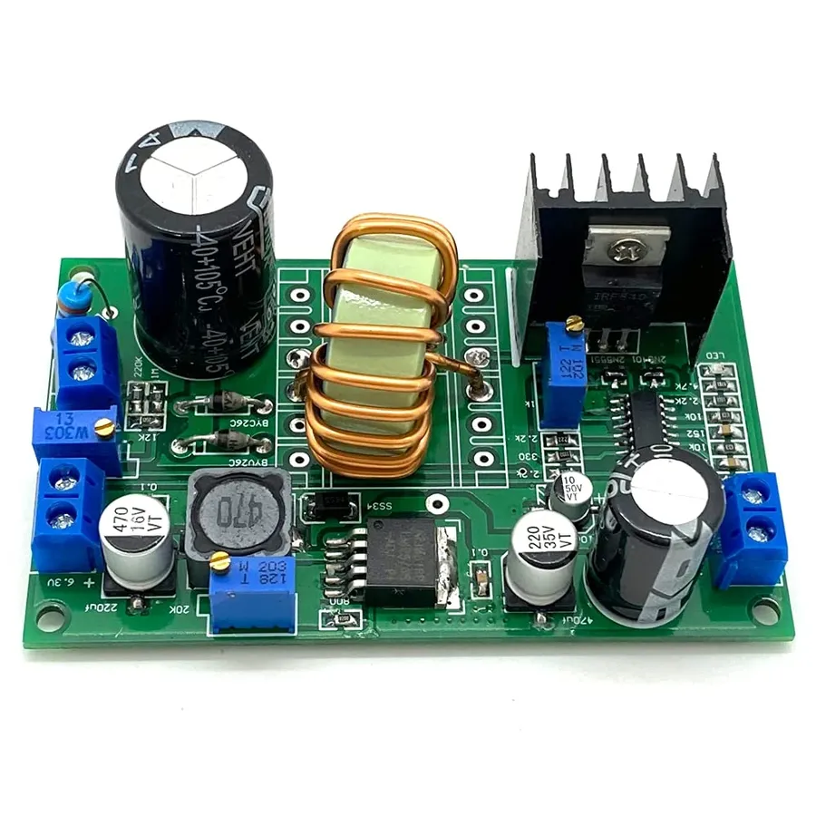
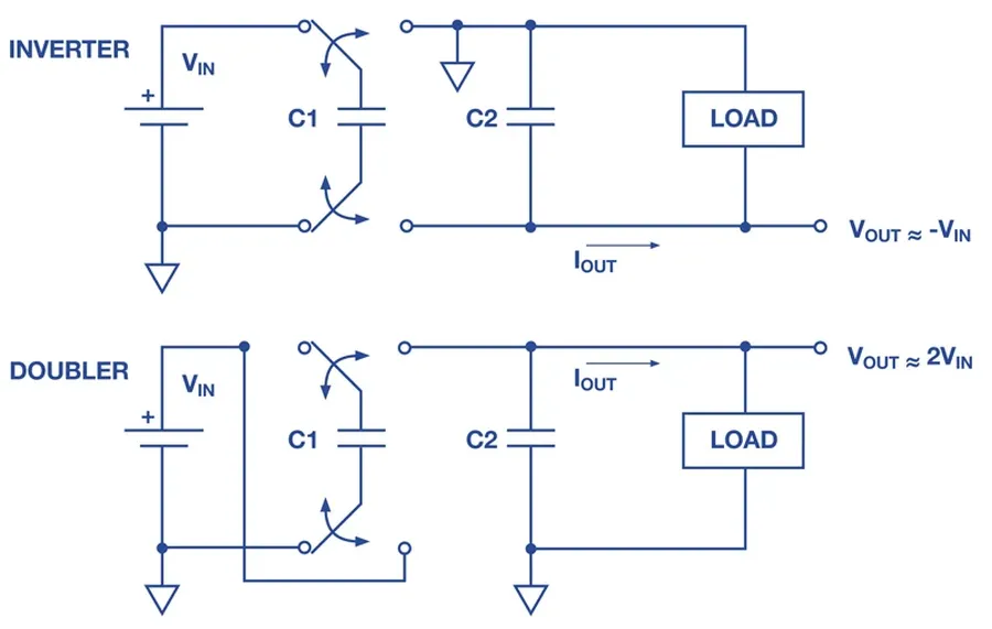
Switched capacitor circuits are adept at manipulating voltage levels, notably through voltage inversion and doubling. These techniques are crucial for power management in portable devices and integrated circuits, where efficient voltage conversion is paramount without using inductors.
In essence, switched capacitor voltage converters operate by transferring charge between capacitors through strategically timed switches. This charge transfer allows for the creation of different voltage levels relative to the input, enabling both voltage inversion and multiplication.
The following sections delve into specific implementations and the underlying operational principles, offering clarity on the practical aspects of switched capacitor based voltage converters.
| Converter Type | Description | Operation | Applications |
|---|---|---|---|
| Voltage Inverter | Creates a negative voltage from a positive input. | A capacitor is charged to the input voltage, then switched to connect to the output with reversed polarity. | Generating negative bias voltages, signal processing circuits that require dual power supplies. |
| Voltage Doubler | Approximately doubles the input voltage. | Two capacitors are charged in parallel, and then switched to connect in series, effectively doubling the voltage. | Providing higher voltage rails for low-power systems and driving LEDs |
This section addresses common inquiries regarding switched capacitor circuits, clarifying their purpose, function, limitations, and applications in analog signal processing. This detailed analysis aims to provide a clear understanding of their implementation and usage, ensuring no doubts remain about their application.
While switched capacitor circuits offer numerous advantages, their practical implementation is subject to various non-ideal effects that can significantly impact performance. These effects arise from the limitations of real-world components and introduce complexities that need to be carefully considered during the design process. Understanding these limitations is crucial for achieving the desired circuit behavior and performance metrics.
| Non-Ideal Effect | Description | Impact on Performance | Mitigation Strategies |
|---|---|---|---|
| Switch Resistance (Ron) | The on-resistance of the MOSFET switches used in the circuit. | Causes incomplete charge transfer, leading to gain errors, reduced bandwidth, and increased settling time. | Using switches with low Ron, employing larger switches, minimizing the number of series switches. |
| Parasitic Capacitance | Unwanted capacitances present between various nodes of the circuit, especially at switch terminals and capacitor plates. | Introduces loading effects, reduces charge transfer efficiency, and contributes to noise and distortion. | Careful layout design, use of guard rings, minimizing the area of connections between components |
| Clock Feedthrough | Coupling of the clock signal from the switch control input to the output. | Introduces unwanted glitches and noise, and causes offset errors in precision circuits. | Using dummy switches, differential topology, optimizing the timing of clock signals, and using switch driving circuitry. |
| Charge Injection | Charge injection occurs when the MOS switch turns off, some charge is injected onto the capacitors during switching, altering the charge stored on the capacitor. | Introduces voltage offsets, causing inaccuracies in gain, comparator offset and filter characteristics. | Use of dummy switches, minimizing channel lengths, differential topology, correlated double sampling. |
| Finite Op-Amp Gain and Bandwidth | The operational amplifiers used to buffer or process the switched capacitor signal have non-ideal gain and bandwidth limits. | Impacts precision and speed, causing nonlinear behavior, settling errors, and reduced signal fidelity. | Selecting high gain-bandwidth op-amps, using a feedback topology to minimize the effects of finite gain. |
| Capacitor Mismatch | Capacitors in ICs are not perfectly matched to their target values. | Causes gain errors and variation in circuit performance due to variations in capacitance values. | Using capacitor arrays for trimming or calibration. |
The trade-off between precision and speed is also a practical consideration. Higher precision often requires slower switching frequencies and larger capacitor sizes, which affect the speed of operation. Design must balance these two factors based on application requirements.
Advanced switched capacitor circuits extend beyond basic implementations, employing sophisticated topologies and techniques to achieve higher performance and meet specialized application requirements. These advancements often involve complex clocking schemes, charge pump architectures, and innovative circuit designs to optimize parameters such as efficiency, noise, and precision.
Switched capacitor circuits, with their unique ability to mimic traditional circuit elements using only switches and capacitors, represent a fundamental building block in modern analog and mixed-signal integrated circuits. From efficient power conversion to precision filtering, the versatility of switched capacitor technology has revolutionized numerous fields. By understanding their underlying principles and practical considerations, we unlock the potential for even more innovative applications, furthering the progress of microelectronics and its impact on society. The journey of switched capacitors continues, promising exciting developments in the future.

