In the realm of electronics, the 13001 transistor often plays a pivotal role, acting as a silent workhorse in numerous devices. From controlling the flow of electricity in simple circuits to powering complex systems, this NPN Bipolar Junction Transistor (BJT) is a key component. This guide will unlock the secrets of the 13001 transistor, exploring its specifications, applications, and how it contributes to the technology that shapes our modern world. Whether you’re a seasoned engineer or just beginning your journey in electronics, you’ll find a wealth of knowledge here about the robust 13001 transistor, a testament to the ingenuity of semiconductor technology.
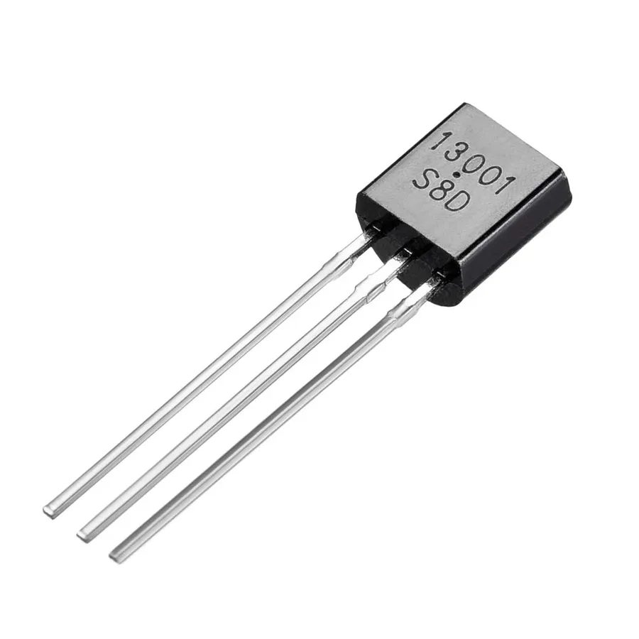
The 13001 transistor is a silicon-based NPN bipolar junction transistor (BJT) primarily designed for high-voltage, medium-current switching applications. Its construction and operational characteristics make it suitable for efficient power control in various electronic circuits, particularly those requiring fast switching speeds.
The core of the 13001 transistor comprises three layers of doped semiconductor material: a thin layer of P-type material (the base) sandwiched between two N-type layers (the collector and emitter). This NPN structure dictates the flow of current; current flows from collector to emitter when a positive voltage is applied to the base relative to the emitter. This behavior is crucial in applications where the transistor is used as an electronic switch, enabling rapid on/off control of power.
The NPN design of the 13001 is favored in switching applications due to its efficiency and ease of control. The NPN transistor's operation relies on minority carrier injection which results in faster switching speeds compared to PNP counterparts. This characteristic of the 13001 allows it to rapidly turn on and off, making it suitable for applications where a fast response to control signals is essential. Further, the ability to easily switch higher voltages and moderate current makes the 13001 extremely versatile in many power electronics applications.
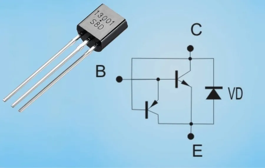
The 13001 transistor, a three-terminal semiconductor device, employs a bipolar junction transistor (BJT) structure, and the precise arrangement of its terminals—the base, collector, and emitter—is fundamental for its proper operation in any circuit. Understanding the function of each pin is crucial for effective circuit design and troubleshooting, as incorrect connections can lead to malfunction or damage.
| Pin | Symbol | Description | Function |
|---|---|---|---|
| Base | B | The control terminal of the transistor | Controls the current flow between the collector and emitter by applying a small current or voltage. |
| Collector | C | The terminal through which current flows into the transistor | Collects the majority of current flowing through the transistor and is typically connected to the load. |
| Emitter | E | The terminal through which current flows out of the transistor | The terminal where current exits the transistor and is often connected to ground or the reference potential. |
The physical pinout of the 13001, typically found in a TO-92 package or similar, requires careful identification to ensure that these functional connections are made correctly. Datasheets, which are readily available from manufacturers, provide detailed illustrations and specifications that are essential for accurate implementation of the 13001 in any circuit design.
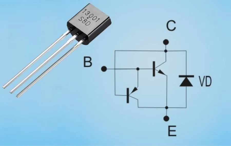
Understanding the electrical characteristics of the 13001 transistor is paramount for effective and safe circuit design. These parameters dictate the device's operational limits and behavior within a circuit. Ignoring these specifications can lead to component damage or circuit malfunction.
| Parameter | Symbol | Typical Value | Unit | Description |
|---|---|---|---|---|
| Collector-Emitter Voltage | VCEO | 400 | V | Maximum voltage that can be applied between the collector and emitter with the base open. |
| Collector-Base Voltage | VCBO | 700 | V | Maximum voltage that can be applied between the collector and base with the emitter open. |
| Emitter-Base Voltage | VEBO | 9 | V | Maximum voltage that can be applied between the emitter and base with the collector open. |
| Collector Current | IC | 1.5 | A | Maximum continuous current the transistor can handle from collector to emitter. |
| Peak Collector Current | ICM | 3 | A | Maximum current the transistor can handle in pulses. |
| Power Dissipation | PC | 30 | W | Maximum power the transistor can dissipate without damage. |
| DC Current Gain (hFE) | hFE | 10-40 | - | Ratio of collector current to base current. |
It's crucial to note that these are typical values and can vary between manufacturers. Always refer to the specific datasheet for your component to ensure you're working within its safe operating area. The values listed in the datasheet represent absolute maximums and should not be exceeded during operation to ensure optimal performance and longevity of the transistor.
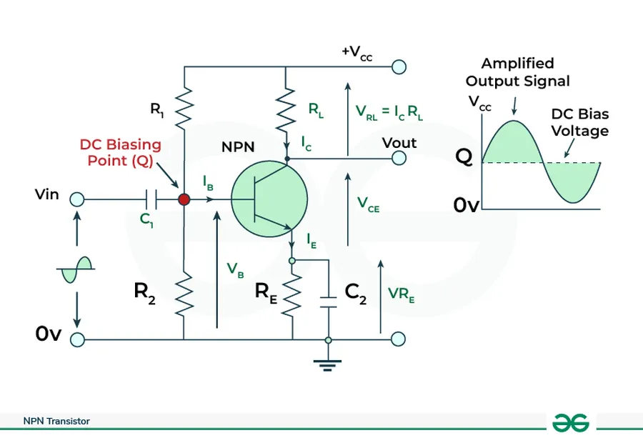
The 13001 transistor, while effective in various switching applications, might not always be readily available or the optimal choice for every design scenario. Identifying suitable equivalents and substitutes is crucial for ensuring design flexibility and maintaining functionality. This section offers a guide to alternative transistors, focusing on those that can serve as direct replacements and highlighting their unique characteristics.
| Transistor | Type | VCEO (V) | IC (A) | PC (W) | Key Differences & Considerations |
|---|---|---|---|---|---|
| 13001 | NPN BJT | 400 | 1 | 5 | High voltage switching, moderate current capability. |
| MJE13001 | NPN BJT | 400 | 1 | 5 | Direct replacement; same electrical characteristics and pinout |
| KSE13001 | NPN BJT | 400 | 1 | 5 | Direct replacement; may have slight variations in manufacturing processes |
| 2SC2625 | NPN BJT | 450 | 3 | 50 | Higher current and power; requires heatsinking; may have a different pinout. |
| 2SC3320 | NPN BJT | 400 | 1.5 | 30 | Moderate current and higher power; different package; check pinout |
| BU406 | NPN BJT | 300 | 3 | 40 | Lower voltage, higher current; consider power dissipation; different pinout |
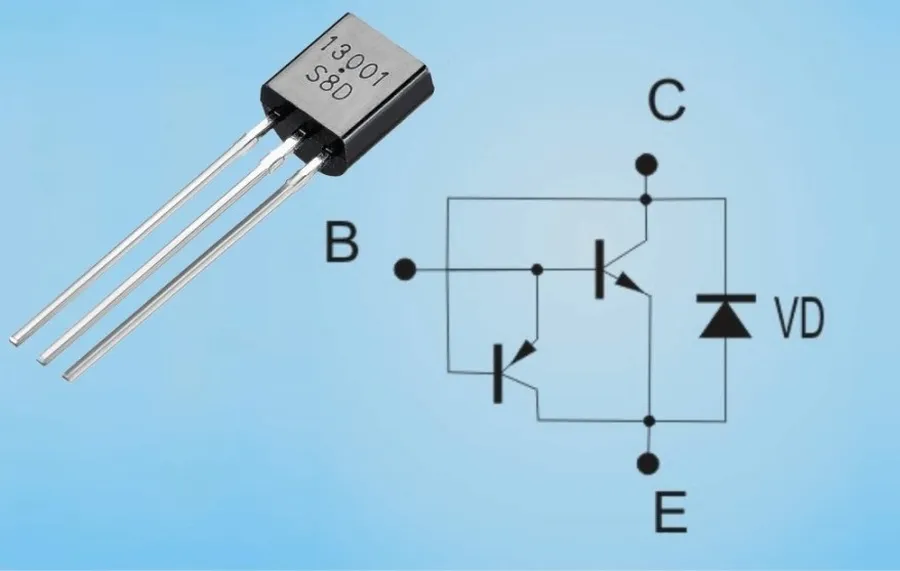
The 13001 transistor, a versatile NPN bipolar junction transistor, finds extensive use in applications requiring moderate current handling at higher voltages. Its design makes it particularly suitable for switching and power control functions, commonly found in various electronic devices.
Specifically, the 13001 transistor is frequently implemented in circuits such as:
These applications exploit the 13001's capability to control power to other devices. When designing with this transistor, it is essential to ensure that the voltage and current requirements of the intended use case do not exceed the transistor's maximum rated values. Proper thermal management is also important as excessive power dissipation can lead to overheating and component failure.
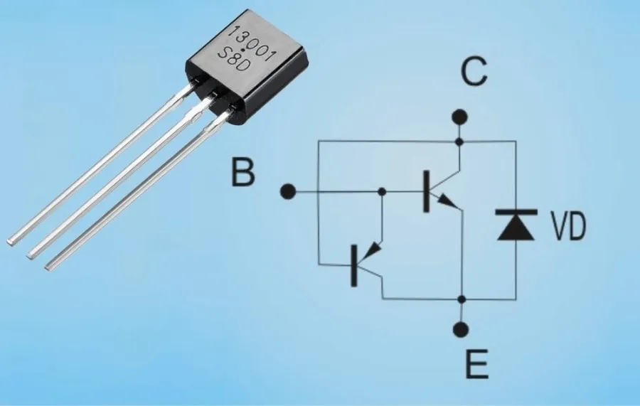
Designing effective circuits with the 13001 transistor requires careful attention to base current limiting, proper biasing, and thermal management to ensure both optimal performance and longevity of the device. These precautions will prevent damage and maximize the transistor's operational lifespan.
This section addresses common inquiries regarding the 13001 transistor, providing concise answers to frequently asked questions. These questions cover the transistor's type, operating characteristics, and typical applications, offering a deeper understanding of its usage.
The 13001 transistor, while effective for specific high-voltage, moderate-current applications, differs significantly from other common NPN transistors like the BC547 and 2N2222. This comparison highlights the trade-offs in choosing the right transistor for a given circuit, considering parameters such as voltage and current ratings, gain, and switching speeds.
| Parameter | 13001 | BC547 | 2N2222 |
|---|---|---|---|
| Polarity | NPN | NPN | NPN |
| Collector-Emitter Voltage (VCEO) | 400V | 45V | 40V |
| Collector Current (IC) | 1A | 0.1A | 0.8A |
| Power Dissipation (PC) | 10W | 0.5W | 0.8W |
| Transition Frequency (fT) | 3MHz | 300MHz | 300MHz |
| Application | High Voltage Switching | General Purpose, Low Current | General Purpose, Medium Current |
The table above demonstrates clear distinctions in key parameters. The 13001 is designed for higher voltage and power handling, making it suitable for applications like power supplies and inverters. The BC547 is a general-purpose transistor that operates at lower voltages and currents. The 2N2222 is a medium power transistor, with a higher current capacity than the BC547.
Key Differences and Considerations:
When selecting a transistor, engineers must carefully weigh these characteristics against the requirements of their specific applications. The 13001's high-voltage capacity makes it unsuitable for low-voltage circuits where components like the BC547 or 2N2222 would be more efficient and appropriate. Conversely, the BC547 would be an inappropriate choice for high-voltage power supply circuit where the 13001 is a better fit. The 2N2222 would be best suited for medium current and medium power applications
The 13001 transistor, a ubiquitous NPN BJT, stands as a testament to the essential role transistors play in modern electronics. From its fundamental structure to its wide array of applications, the 13001 continues to be a critical component in a variety of electronic devices. This guide has explored its key characteristics, pinout, equivalent alternatives, and common uses. As technology advances, it's crucial to understand and appreciate how such fundamental building blocks like the 13001 transistor facilitate the electronic innovations that power our world. Whether for switching or amplification, the 13001 transistor remains a vital and versatile tool in the electronics engineer's toolkit, promising even more interesting applications in the years ahead.

