Just like the intricate patterns found in nature, circuit board patterns are the blueprints of our modern electronics, enabling the flow of electricity to power the devices we use every day. This article will delve into the world of circuit board patterns, unraveling their complexities and revealing their crucial role in technology. We will explore their visual representation, design rules, and impact on the functionality of electronic devices, all while highlighting the crucial role of circuit board patterns in modern technology. We'll explore not just what they are, but why they are designed the way they are, offering insights into the fascinating world of micro-electronics.

Circuit board patterns are the intricate visual blueprints that dictate the layout and electrical connections on a printed circuit board (PCB). These patterns, typically composed of conductive traces (lines), pads for component mounting, and vias (interlayer connections), form the physical embodiment of an electronic circuit's design, establishing the pathways for electrical signals and power distribution. The precision and accuracy of these patterns directly impact the functionality, performance, and reliability of the final electronic device.
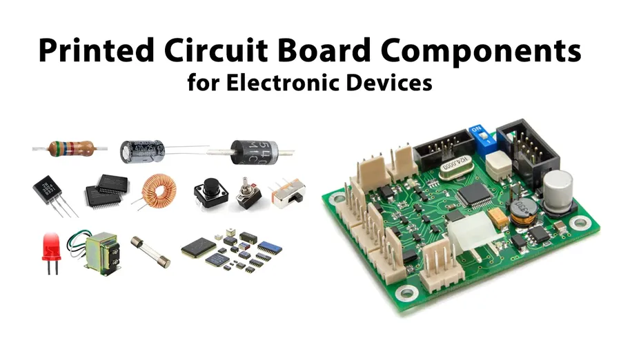
Circuit board patterns are fundamental to the functionality of virtually all electronic devices. These patterns, comprising conductive traces, pads, and vias, dictate the flow of electrical signals and power throughout the system. Their precise design is paramount as they directly influence signal integrity, power distribution, and overall system reliability.
The significance of these patterns extends beyond mere connectivity; they are integral in maintaining the desired electrical characteristics for optimal performance. Errors or inadequacies in pattern design can manifest as signal distortion, power fluctuations, and ultimately, device failure. Therefore, the process of designing, verifying, and fabricating circuit board patterns is critical in the electronics industry.
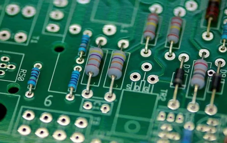
Circuit board patterns are constructed from several fundamental elements, each playing a crucial role in the overall functionality of the electronic circuit. These elements include traces, vias, pads, and planes. Understanding their individual characteristics and functions is essential for effective PCB design.
| Element | Description | Function |
|---|---|---|
| Traces | Conductive pathways, usually thin lines of copper, that route electrical signals. | Carry signals and power between components. |
| Vias | Small plated through-holes that create connections between different layers of a multilayer PCB. | Facilitate vertical connections and signal routing between layers. |
| Pads | Exposed metal areas to which electronic components are soldered or connected. | Provide solder points for component mounting. |
| Planes | Large areas of solid copper, often used as power or ground planes. | Provide power distribution, ground connections, and shielding. |
The interplay and precise arrangement of these elements dictate the electrical behavior of the circuit. Careful consideration of their properties, such as trace width for impedance control, via size for current handling, and plane shape for effective power distribution and shielding, is paramount in ensuring a functional and reliable circuit board.
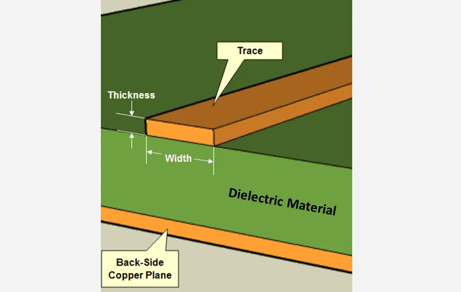
Effective circuit board design hinges on adherence to fundamental principles that ensure functionality, reliability, and performance. These principles encompass various aspects, including impedance control, trace geometry, power distribution, and signal integrity. A thorough understanding of these rules is crucial for engineers to create efficient and robust electronic devices.
| Design Principle | Description | Importance |
|---|---|---|
| Impedance Control | Maintaining a consistent impedance along signal traces to prevent reflections and signal loss. | Critical for high-speed signal transmission and maintaining signal integrity. Mismatched impedances can lead to signal distortion and errors. |
| Trace Width and Spacing | Determining the width of traces and the spacing between them based on signal current, impedance, and manufacturing capabilities. | Impacts impedance, current carrying capacity, and reduces crosstalk. Sufficient spacing avoids shorts and ensures proper isolation. |
| Power Distribution | Designing efficient power planes and traces to deliver stable and clean power to the various components of the circuit. | Ensures components receive adequate power without voltage drops. Proper power distribution reduces noise and thermal issues. |
| Minimizing Signal Interference | Employing techniques to minimize crosstalk and electromagnetic interference (EMI) between signal traces. | Reduces the impact of noise and prevents signal degradation. Strategies include shielding, trace routing, and ground plane optimization. |
| Grounding Strategy | Establishing proper ground connections to ensure signal return paths, minimizing noise and improving signal quality. | Ensures a stable reference point for all signals, preventing ground loops and reducing the impact of common-mode noise. |
| Thermal Management | Designing the circuit board layout to facilitate heat dissipation, preventing overheating and ensuring component reliability. | Crucial for components that generate heat. Adequate thermal management improves component lifetime and overall system stability. |
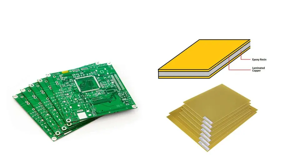
Circuit board patterns, the very essence of electronic connections, manifest in various forms, each tailored to specific application needs and complexities. These patterns dictate the flow of electrical signals and the physical connections of components. The selection of the appropriate type is crucial to the functionality and performance of electronic devices.
| Pattern Type | Description | Applications | Advantages | Disadvantages |
|---|---|---|---|---|
| Single-Sided | Traces and components on one side of the board. | Simple circuits, educational projects, basic consumer electronics. | Low cost, easy to manufacture. | Limited routing, not suitable for complex designs. |
| Double-Sided | Traces and components on both sides of the board. | Intermediate complexity devices, common in many applications. | Increased density, better routing flexibility. | More complex than single-sided, slightly higher cost. |
| Multilayer | Multiple layers of conductive material separated by insulating layers. | High-density electronics, complex circuitry, advanced applications. | Extremely high density, complex routing, enhanced functionality. | Higher cost, more complex to manufacture, longer lead time. |
| Flexible (Flex) | Circuits built on flexible substrate, bendable and adaptable. | Portable devices, wearables, applications requiring flexibility. | Lightweight, flexible, adaptable to various shapes. | Higher manufacturing cost, more fragile than rigid boards. |
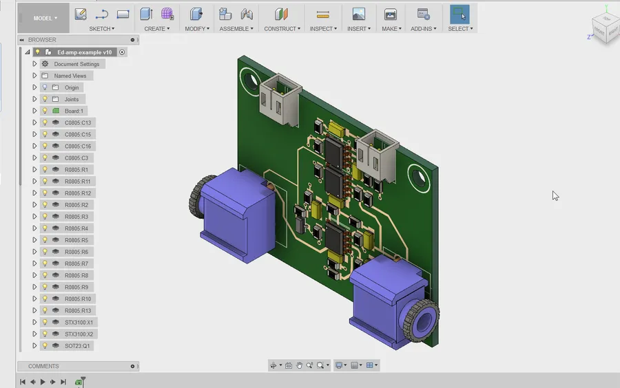
The design and manipulation of circuit board patterns rely heavily on specialized software and design tools. These tools have revolutionized the process, enabling engineers to create intricate and precise layouts with enhanced efficiency and accuracy, and are indispensable for modern electronic product development. These tools not only automate complex tasks but also offer features for simulation and verification, ensuring designs are manufacturable and functional before physical prototyping.
Below are some of the key features and functionalities of these tools:
Here's a comparison of some popular circuit board design software packages, highlighting their strengths and weaknesses:
| Software | Strengths | Weaknesses | Cost |
|---|---|---|---|
| Altium Designer | Comprehensive feature set, excellent routing, strong community support. | High cost, steep learning curve for beginners. | High |
| KiCad | Open source, free to use, actively developed, good for hobbyists. | User interface not as polished as commercial options, may require additional setup. | Free |
| Eagle (Autodesk) | Popular among hobbyists and small businesses, good online support, accessible price point. | Feature set not as extensive as high-end options, large designs can be slow. | Moderate |
| OrCAD (Cadence) | Powerful simulation tools, widely used in industry, capable of complex designs. | High cost, can be difficult to master for simple projects. | High |
| PADS Professional (Siemens) | Highly scalable for large-scale enterprise designs, advanced signal integrity analysis. | Very high cost, targeted at large companies, overkills for simple tasks. | Very High |
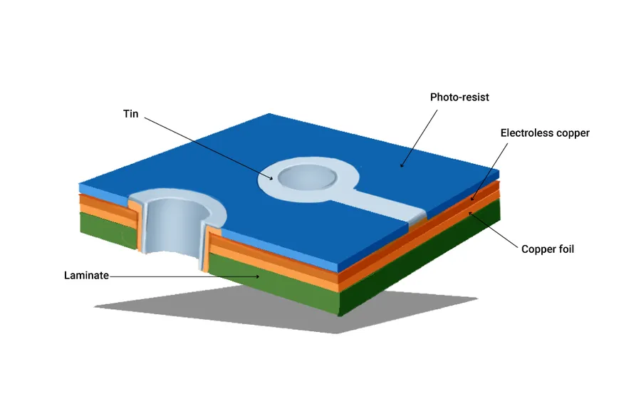
The fabrication process transforms meticulously designed circuit board patterns into physical printed circuit boards (PCBs). This multi-stage process demands high precision to ensure the final product accurately reflects the design, guaranteeing the intended electrical performance. Key steps include etching, drilling, and plating, each requiring careful control and execution.
The fabrication process typically involves the following sequential stages:
The precision required in each of these steps cannot be overstated. Any deviation can lead to a non-functioning board, making careful adherence to the design specifications and manufacturing tolerances paramount. Advancements in fabrication technologies constantly drive improvements in accuracy and efficiency, enabling the manufacture of increasingly complex and high-density PCBs.
This section addresses common questions regarding circuit board patterns, offering concise and precise answers to enhance understanding of PCB design and manufacturing.
The evolution of circuit board pattern design is being propelled by the increasing complexity and miniaturization of electronic devices. Future trends are geared towards addressing the demands for higher performance, greater density, and enhanced flexibility in electronic circuits.
Circuit board patterns are indeed the unsung heroes of modern technology. They are the intricate maps of our electronic devices, essential for efficient functionality and reliability. From the simple lines connecting components to the sophisticated designs found in complex devices, understanding these patterns offers insights into the heart of electronics. As technology advances, these patterns will only become more crucial, showcasing the ongoing evolution of circuit board design. Just as natural patterns reflect underlying processes, so do circuit board patterns—revealing the sophisticated interplay of technology. The future of electronics hinges on continued innovation in this foundational element.

