Introduction: As electronics move toward miniaturization, laser solder joints are becoming smaller and harder to inspect. This guide covers four optical detection methods used to evaluate solder joint quality—laser triangulation, reflection distribution, multi-angle imaging, and multi-focus detection—and explains how process control from SPI to 3D AOI prevents defects at the source.
Description: Based on AnyPCBA's small-to-medium volume PCBA manufacturing experience, this guide explains how to inspect laser solder joints using four optical detection methods—and how process control (SPI, 3D AOI, X-Ray) and DFM review prevent soldering defects before they happen.
As 5G deployment continues and precision microelectronics, aerospace, and other industrial fields advance, electronic components are becoming increasingly miniaturized, thinner, and lighter. Precision requirements are rising, and laser soldering—one of the most common processes in the microelectronics industry—must meet increasingly stringent standards for solder quality.
Inspecting PCBs after soldering is critical for both manufacturers and customers. Without proper inspection, performance failures are likely to occur, affecting product sales and company reputation.
Because laser solder joints are often extremely small and difficult to see with the naked eye, how do we efficiently and accurately inspect their quality? This article covers four optical detection methods commonly used in electronics manufacturing, combined with AnyPCBA's manufacturing perspective on ensuring soldering reliability.
Laser soldering offers a small heat-affected zone, minimal deformation, and high efficiency. But in micro solder joints, hidden defects such as cold joints, insufficient solder, and uneven joint surfaces can occur. In high-density, high-precision PCBA, traditional visual inspection is completely inadequate.
This is why optical and machine vision technologies are required.
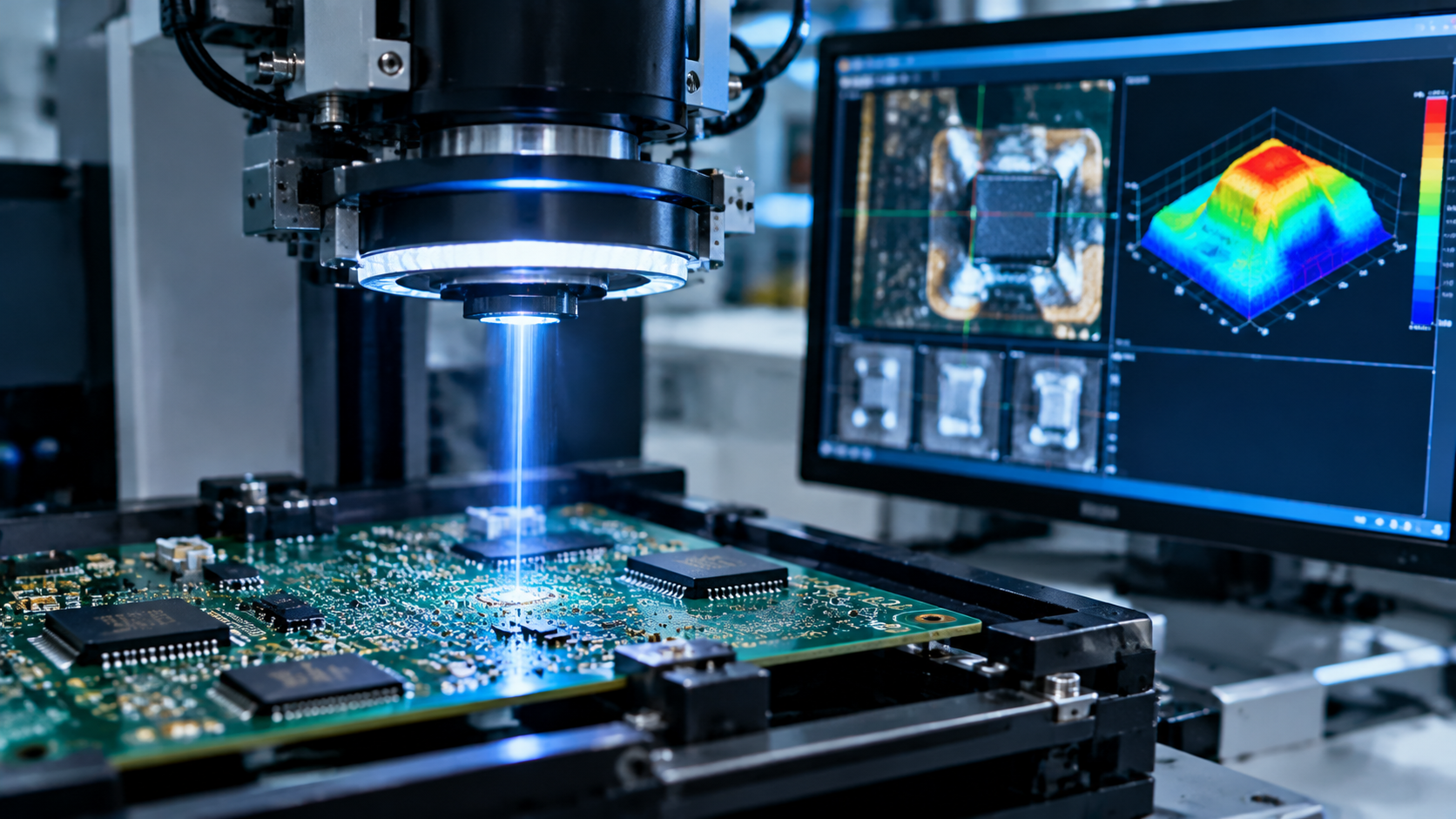
AOI (Automated Optical Inspection) and 3D inspection equipment typically use the following optical principles to capture the 3D topography of solder joints.
Principle: This is the most common method for inspecting 3D shapes. The equipment projects a laser onto the solder joint. Because different surface topographies reflect light at different angles, sensors receive the reflected light and calculate the joint's cross-sectional shape.
Advantages: Based on light scattering principles, it can rapidly build a 3D profile and is suitable for most standard solder joints.
Limitations: If the soldered surface is very smooth and approaches a "mirror" condition, the reflected light becomes too concentrated, reducing measurement accuracy. This requires special attention with certain solder surface finishes.
Principle: Light is projected onto the solder joint from an oblique angle, and a high-resolution camera (such as a TV camera) captures the image from above. By analyzing the reflected light distribution under different angles, the surface slope of the solder can be determined.
Advantages: Particularly suitable for inspecting solder fillet shapes (such as wetting angles).
Limitations: Extremely high requirements for light source uniformity and color control; multiple light sources must work together to capture angular information.
Principle: Uses an inspection device equipped with multiple cameras (at least five) and multiple LED lighting arrays to capture multiple images from different angles.
Advantages: Highly reliable. Eliminates blind spots caused by shadows or reflections from a single angle, making it especially suitable for boards with tall components.
Principle: For ultra-high-density boards, the first three methods may not resolve final results. This technology sets multiple focal planes along the Z-axis (e.g., 10 focus plane detectors). By finding the maximum output, the focus plane is determined, directly measuring solder surface height.
Advantages: Achieves extremely high precision and can even inspect 0.3mm pitch fine-pitch leads.
In AnyPCBA's daily production, for miniaturized and high-density PCBA (such as HDI and rigid-flex boards), we never rely on a single post-solder inspection step.
3.1 Pre-Solder Control (SPI)
If solder paste printing is uneven, even perfect laser or reflow soldering is futile. Before placement, AnyPCBA uses SPI (Solder Paste Inspection) to control paste thickness and area, reducing cold joints at the source.
3.2 Combined 3D AOI and X-Ray
For visible solder joints, we use 3D AOI equipment (using triangulation or focus methods described above) to rapidly scan for insufficient solder, bridging, and tombstoning. For BGA, QFN, and other hidden joints, we use X-Ray for internal inspection.
3.3 DFM-Level "Poka-Yoke" Design
The best inspection is the inspection you don't need. During DFM review, AnyPCBA engineers check whether pad sizes are reasonable, whether stencil apertures will cause solder balls, and whether component spacing will cause shadowing. Resolving these issues at the design stage dramatically improves first-pass yield (FPY) in production.
In microelectronics manufacturing, laser solder joint quality directly determines product lifespan. Whether using triangulation or multi-focus detection, the goal is to see the true condition of the solder joint at micron-level resolution.
For companies, however, choosing a manufacturing partner who understands not only optical inspection but also process control and DFM prevention is the key to ensuring product quality.
AnyPCBA focuses on small-to-medium volume PCB and PCBA manufacturing from 5 to 5,000 pieces, with extensive experience in medical electronics, industrial control, and other high-reliability fields. We are equipped with high-precision 3D AOI, X-Ray, and SPI equipment, and we identify soldering risks during DFM review before production begins.
If you're working on a high-density PCBA project, contact us through our website.