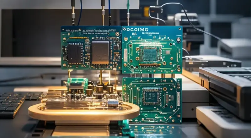
Introduction: As PCBs shrink and component density increases, manual visual inspection is no longer enough. AOI (Automated Optical Inspection) uses high-resolution cameras and image processing to catch missing components, misalignments, and solder defects right on the SMT line. This guide covers how AOI works, what it can detect, and how manufacturing process control prevents the most common SMT defects.
Description: Based on AnyPCBA's small-to-medium volume PCB and PCBA manufacturing experience, this guide explains AOI inspection in SMT production—what it detects, the factors affecting its performance, and how process control from SPI to reflow profile prevents common soldering defects.
In SMT (Surface Mount Technology) production, as circuit boards shrink and component density increases, manual visual inspection is no longer sufficient to guarantee quality. AOI (Automated Optical Inspection) has emerged as an indispensable gatekeeper on the modern SMT production line.
This article explains how AOI works, what it can detect, its limitations, and how to reduce SMT defects through process control.
AOI uses high-resolution cameras and image processing technology to inspect the placement position of PCB components, solder joint shapes, and the presence of solder paste defects.
Core reasons for using AOI:
Addressing high-density challenges: Manual inspection is no longer capable of checking 0201 and 01005 micro-components and dense pin arrays.
Identifying defects early in the assembly process: AOI catches problems immediately after placement and reflow, preventing defective boards from moving further down the line.
Reducing repair costs: Finding and repairing defects on the line is far cheaper than disassembling a finished product.
Depending on the working method, AOI can be divided into inline AOI (real-time inspection on the production line) and offline AOI (sampling or full inspection of boards that have already come off the line).
AOI's detection capabilities are extensive, covering both component-level and solder joint-level issues.
AOI covers virtually all common packages, including:
Rectangular/cylindrical chip components (0805 and larger), tantalum capacitors, inductors, transistors, and resistor arrays.
QFP and SOIC (0.4mm pitch and larger), connectors.
Irregular/odd-form components.
Main detectable defects include:
Extra, missing, or wrong components (wrong part placement)
Tombstoning, side-standing, partial lifting, reversed placement, and polarity errors
IC lead bending and lifted leads
Text recognition (silkscreen clarity)
Excess solder, insufficient solder, or no solder
Cold joints and solder bridging
Solder balls and lifted joints
Cracked solder joints
AOI is powerful, but not perfect. Its inspection effectiveness is influenced by external and internal factors:
External factors: placement quality, flux content, component condition, room temperature, and soldering quality.
Internal factors: AOI lighting, machine internal temperature, image analysis algorithms (which determine whether it can recognize defects against complex backgrounds), mechanical system, and camera temperature.
When AOI triggers an alarm, blindly reworking the board without addressing the root cause means the defect will recur. Here are the five most common defects encountered on AnyPCBA's production line and how to solve them.
Causes: incorrect placement position; insufficient solder paste or insufficient placement pressure; excessive flux content in the solder paste causing component movement during reflow.
Solutions: Calibrate placement coordinates; increase solder paste volume and placement pressure; switch to solder paste with lower flux content.
Causes: solder paste slump; excessive solder paste; overly fast heating rate.
Solutions: Increase metal content or viscosity of the solder paste; reduce stencil aperture and increase squeegee pressure; adjust the reflow temperature profile.
Causes: poor solderability of pads and components; incorrect printing parameters (such as squeegee pressure and speed); improper reflow temperature and ramp rate.
Solutions: Strengthen incoming inspection of PCBs and components; calibrate printing parameters; re-adjust the reflow temperature profile.
Causes: placement offset; flux in the solder paste causing the component to lift; insufficient solder paste thickness; uneven and overly fast heating.
Solutions: Adjust printing parameters; use solder paste with less flux; increase solder paste thickness; adjust the temperature profile; switch to Ag-containing solder (such as SAC305).
Causes: insufficient solder paste; poor solderability of pads and components; short reflow time.
Solutions: Enlarge stencil apertures; use higher-quality solder paste or re-dip the component; extend reflow time.
As a factory focused on small-to-medium volume PCB and PCBA manufacturing, AnyPCBA understands exactly where AOI fits in the overall quality control chain.
Our manufacturing capabilities cover 2 to 64 layers, including HDI, rigid-flex, and high-frequency hybrid. We hold ISO 13485 (medical) and IATF 16949 (automotive) certifications.
On our production line, AOI is not an isolated step. It works together with the following processes:
SPI (Solder Paste Inspection): inspecting solder paste printing quality before placement to eliminate insufficient solder, excess solder, and bridging at the source.
High-precision placement machines: ensuring accurate placement coordinates and pressure to reduce shift and tombstoning.
Customized reflow profiles: tailoring temperature profiles for different boards and components (especially heat-sensitive ones) to reduce cold joints caused by thermal stress.
X-Ray inspection: for BGA, QFN, and other hidden solder joints that AOI cannot see, X-Ray inspection verifies internal joint quality.
Our engineers confirm pad design, stencil apertures, and panelization during DFM review to reduce defects that would trigger AOI alarms at the source. If AOI identifies an issue, our engineering team traces it back to the process root cause—rather than simply reworking the board.
If you're working on an SMT assembly project, or want to learn more about our quality inspection process, contact us through our website.