Introduction: In PCB design, holes are not all created equal. Plated through holes (PTH), vias, and non-plated through holes (NPTH) serve completely different purposes. Mislabeling them in design files often leads to manufacturing delays, extra costs, or assembly failures. This guide explains the differences and the manufacturing pitfalls to avoid.
Description: Based on AnyPCBA's small-to-medium volume PCB and PCBA manufacturing experience, this guide clarifies the definitions of PTH, vias, and NPTH, and explains how DFM review catches hole-related design issues—such as via treatment and annular ring clearance—before production.
In PCB design and manufacturing, there are many types of holes. It is common for beginners to confuse Plated Through Holes (PTH), Non-Plated Through Holes (NPTH), and Vias.
If hole properties are not clearly defined in the design files, the factory may use standard processes that result in boards that cannot be assembled or that suffer from short circuits.
This article clarifies the differences between these hole types from an engineering and manufacturing perspective, and highlights the key points to watch out for during design.
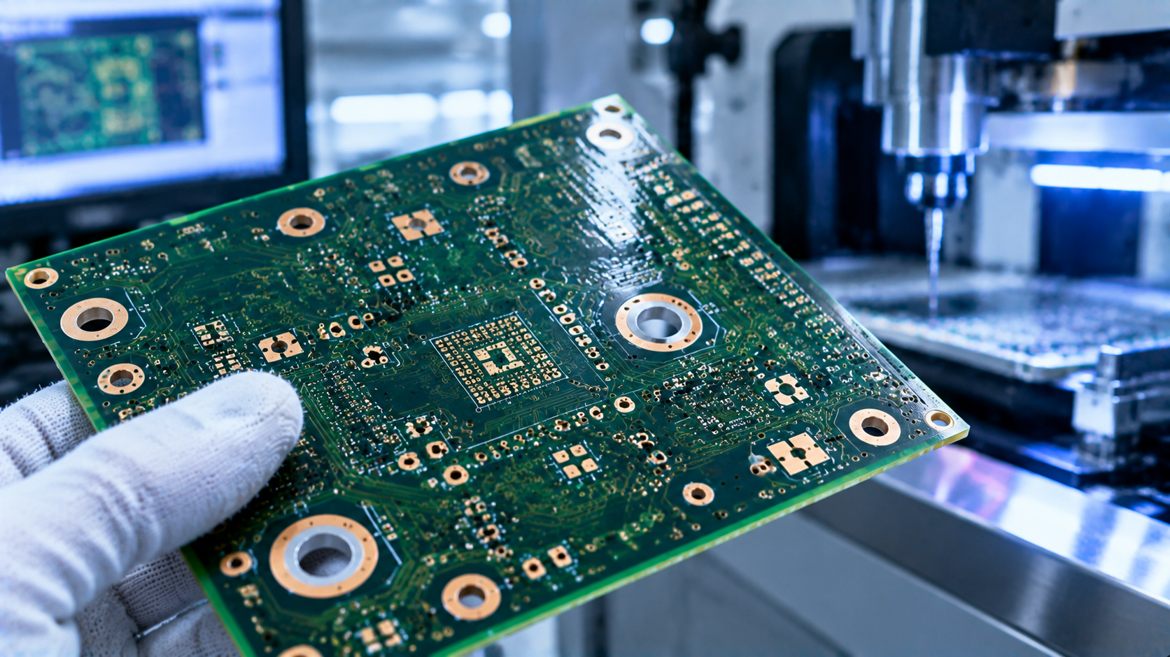
A Plated Through Hole (PTH) is a hole in which a metal layer (usually copper) is formed on the hole wall through electroplating or chemical plating during PCB manufacturing. This metal layer makes the hole conductive.
Characteristics of PTH:
Conductivity: The metal layer on the hole wall allows current to flow from one layer to another.
Reliability: Provides good electrical connection, enhancing PCB reliability.
Cost: Because it requires an additional plating process, PTH costs are usually higher than NPTH.
Manufacturing process: Involves complex electroplating or chemical copper deposition.
Applications: Commonly used in multilayer PCBs for electrical connections between inner layers, or for soldering through-hole components.
Advantages of PTH:
Multilayer connection: Enables electrical connections between multiple PCB layers for complex circuit designs.
Signal integrity: Provides a good conductive path, helping maintain signal integrity.
Current carrying capacity: Can carry larger currents, suitable for high-power applications.
Disadvantages of PTH:
Cost: Higher manufacturing cost.
Manufacturing complexity: Requires precise control of the plating process and uniform hole wall thickness.
Diameter variation: Plating can affect the hole diameter, influencing high-density routing.
Important note: In industry standards, a via is actually a subcategory of PTH.
A via specifically refers to a plated hole used only for interlayer electrical connection. Vias are not used for inserting component leads (because they are too small). In modern PCBs, the most common via is the through via, followed by blind vias, buried vias, and microvias.
Characteristics of Vias:
Pure electrical connection: Vias route signals from one layer to another and cannot be used for soldering components.
Small size: Via diameters are usually much smaller than component mounting holes (typically between 0.2mm and 0.45mm).
Usually tented or plugged: To prevent solder from flowing into the via and causing shorts or wicking, designs typically require the factory to tent or plug vias.
Advantages of Vias:
Space saving: Small size enables fanout under high-density packages like BGAs.
Routing flexibility: Allows traces to route through multiple layers.
Disadvantages of Vias:
Increased manufacturing difficulty: Microvias (laser-drilled) and blind/buried vias are very expensive.
Signal integrity issues: Vias introduce parasitic capacitance and inductance. In ultra-high-speed circuits, via stubs cause signal reflection, sometimes requiring back drilling.
If vias are a type of PTH, what is the hole that "has no metal layer on the wall and is used for physical mounting"? The answer is: Non-Plated Through Hole (NPTH).
NPTH has no copper layer on the hole wall. Its primary purpose is mechanical mounting (such as for screws or locating posts) or providing thermal channels.
Characteristics of NPTH:
Non-conductive: No copper on the hole wall; cannot be used for electrical connection.
Lower cost: No plating required; only mechanical drilling.
Applications: Commonly used for mounting holes in single-sided, double-sided, or multilayer PCBs.
During DFM review at AnyPCBA, we frequently encounter manufacturing issues caused by unclear hole property definitions:
1. Unclear annular ring and anti-pad dimensions
If a PTH is routed too close to a plane layer (such as GND) without a sufficiently large anti-pad, drilling can cause short circuits between the annular ring and the plane. The factory will confirm the inner-layer isolation ring dimensions with you.
2. Via treatment not specified (tented vs. plugged)
If a via is in a BGA pad (via-in-pad), it must be explicitly marked for resin plugging and plated flat; otherwise, solder will wick through the hole during reflow. If it is a standard signal via, tenting is sufficient. If the file does not specify, the factory will default to the cheapest tenting option, which may cause soldering defects later.
3. NPTH (mounting holes) mistakenly marked as PTH
If a mounting hole is designed as a PTH, the factory will spend extra process steps on plating, increasing costs. If the screw needs to be grounded, it must be made as a PTH. This must be explicitly marked on the drawings.
As a factory focused on small-to-medium volume PCB and PCBA manufacturing, AnyPCBA has accumulated years of experience in hole processing and process control.
Our manufacturing capabilities cover 2 to 64 layers, supporting conventional mechanical drilling, laser microvias, HDI blind/buried vias, and resin plugging and copper paste plugging. We hold ISO 13485 (medical) and IATF 16949 (automotive) certifications.
During DFM review, we focus on hole-related design checks:
Clear hole properties: which are PTH, which are NPTH, and which are vias
Via dimensions and annular ring: confirming the ratio of via diameter to pad/annular ring meets process capabilities
Via treatment: whether plugging, tenting, or opening is required
Hole-to-trace spacing: confirming the distance from the hole wall to surrounding traces is sufficient to avoid ring breakage
High-density BGA fanout: confirming the process feasibility of microvias or laser vias
Our engineers help you confirm these critical details at the design stage, so your boards are not only drawable, but stable and reliable to produce.
If you're working on PCB design, or have questions about hole processes, contact us through our website.