Introduction: Power PCBs face challenges that standard signal boards don't: high currents, high voltages, and extreme heat. This guide covers the core essentials of power PCB design—thermal management, power and ground routing, component layout, via design, protection circuits, and EMC—while highlighting the manufacturing pitfalls that can cause production failures.
Description: Based on AnyPCBA's small-to-medium volume PCB and PCBA manufacturing experience, this guide explains power PCB design essentials—from thermal management and current capacity to via design and manufacturability—and how DFM review catches power-related risks before production.
Power PCB design is critical to ensuring the efficient and stable operation of electronic devices. Unlike standard signal boards, power boards (such as power modules, motor drives, and inverters) must not only handle signal logic but also confront the physical challenges of high current, high voltage, and high heat.
This article systematically outlines the core essentials of power PCB design, combined with AnyPCBA's manufacturing perspective, to help engineers avoid the pitfalls that cause production failures.
Power devices generate significant heat during operation, making thermal management the primary task in power PCB design.
Thermal structures: Design appropriate thermal structures such as heatsinks and heat pipes to improve heat conduction efficiency.
Copper layout: Increase the copper area beneath power device pads to improve thermal conductivity and reduce copper resistance. Use thermal via arrays when necessary to conduct heat to the backside or inner layers.
Thermal isolation: Place thermal isolation bands between high-heat devices (such as MOSFETs and inductors) and sensitive components (such as control chips and crystals) to prevent heat radiation from causing control circuit failure.
Power path: Optimize the power path to reduce parasitic resistance and inductance on traces, lowering voltage drop and ripple.
Decoupling capacitors: Place appropriate decoupling capacitors (such as large tantalum capacitors in parallel with high-frequency MLCCs) on power lines to filter high-frequency noise.
Ground design: Use dedicated ground planes in multilayer boards for low-impedance return paths. For high-current switching loops, use star grounding or single-point grounding to reduce ground loop area.
Power boards are extremely sensitive to parasitic inductance and capacitance. Layout and routing directly determine EMI and efficiency.
Minimize the power loop: Power components (switching devices, inductors, input/output capacitors) must be placed extremely close together to ensure the high-frequency switching current loop area is minimized.
Keep sensitive components away: Control chips and feedback traces must be kept away from high dv/dt and high di/dt nodes.
Symmetrical layout: For multi-phase parallel circuits, maintain a symmetrical component layout to reduce circulating currents and electromagnetic interference.
Trace width: Calculate appropriate trace width based on current (e.g., 1oz copper, 1mm trace width carries approximately 2A at 10°C temperature rise) and material characteristics to avoid overheating or excessive voltage drop. Use copper pours instead of traces for high-current paths.
Trace length: Minimize high-current trace length to reduce parasitic inductance.
Avoid right angles: Avoid 90-degree right-angle routing. Use 45-degree angles or rounded transitions to reduce electromagnetic radiation from high-frequency signals.
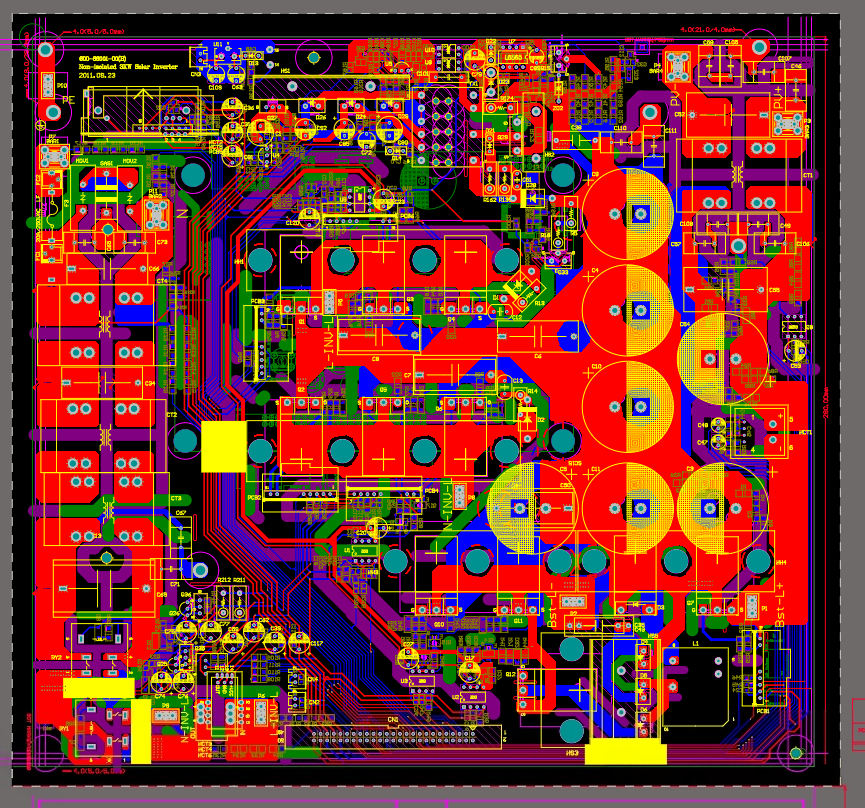
Power PCB layout showing extensive copper pours and heavy vias to handle high current and improve thermal dissipation.
Increase current capacity: Use multiple parallel vias (such as at power layer transitions) where higher current carrying capacity is needed.
Via layout: Arrange vias reasonably to improve power and ground connection stability and reduce via inductance.
Overcurrent and short-circuit protection: Design overcurrent protection circuits (such as fuses and current sense resistors) and short-circuit protection to prevent device damage.
Overvoltage protection: Use metal oxide varistors (MOVs) or transient voltage suppressors (TVS) for overvoltage protection.
Ensure transmission line characteristic impedance matches the source and load.
Reduce crosstalk by increasing trace spacing and using ground plane isolation.
Reduce signal reflection through termination matching.
Shielding design: Shield high-radiation sources (such as power inductors) to reduce electromagnetic interference.
Filters: Use filters on power lines and signal lines to remove conducted noise.
Layer count: Choose the appropriate PCB layer count based on design requirements. Power boards should use at least 4 layers to ensure a complete ground plane.
Stack-up optimization: Optimize the stack-up structure to improve electromagnetic compatibility and thermal performance (such as placing power and ground layers adjacent).
Material selection: Choose high-thermal-conductivity materials (such as heavy copper boards and high-Tg laminates) to improve heat dissipation; choose low dielectric constant and low loss tangent materials to meet electrical requirements.
Mechanical stress: Consider mechanical stress the PCB may experience during assembly and use (such as connector insertion and heatsink mounting).
Environmental factors: Consider the effects of temperature, humidity, vibration, and other factors on PCB performance.
During DFM review at AnyPCBA, we frequently see power designs that look perfect in software but encounter the following challenges at the factory:
1. Conflict between thermal pads and thermal relief
Many engineers connect power transistor thermal pads directly to large copper areas to maximize heat dissipation, without any thermal relief. During wave soldering or reflow, the large copper area absorbs heat rapidly, preventing the pad from reaching soldering temperature and causing cold joints.
AnyPCBA recommendation: For wave soldering, use cross-shaped thermal relief pads for large ground pads. For reflow soldering, increase stencil openings or use bottom-side preheating.
2. Underestimating current-carrying capacity of large-current traces
Some designs use thin traces for high current or too few vias for layer transitions. When the factory builds to the drawing, testing reveals severe trace heating or blistering.
AnyPCBA recommendation: For heavy copper (2oz and above) or high-current designs, always confirm the etching undercut with the factory during DFM review, because heavy copper etching tolerances can reduce actual trace width. Increase via count at high-current nodes.
3. Handling of thermal vias
If a thermal via array is used but not explicitly specified as "resin plugged and plated over," solder paste will wick through the vias during soldering, causing poor solder joints.
AnyPCBA recommendation: Clearly specify the process properties of thermal vias in the drawings. AnyPCBA supports high-density thermal via plugging to ensure a flat surface for both heat dissipation and soldering.
Power PCB design is a complex process that requires designers to possess deep professional knowledge and rich practical experience. Following the essentials above helps engineers design high-performance, reliable power PCBs, providing a solid foundation for stable operation of electronic equipment.
AnyPCBA focuses on small-to-medium volume PCB and PCBA manufacturing from 5 to 5,000 pieces, with extensive experience in industrial power supplies, motor drives, automotive electronics, and other high-power applications.
Our manufacturing capabilities cover 2–64 layers, supporting heavy copper (2–20oz), HDI, and high-frequency hybrid. Our engineers get involved at the DFM review stage to help you anticipate risks related to high current, thermal management, and special processes.
If you're working on power PCB design, or want to learn more about our heavy copper and high-power manufacturing capabilities, contact us through our website.