Blog

PCB Terminology Every Engineer Should Know: From Stack-Up to Solder Mask

Understanding PCB terminology is essential for hardware engineers, procurement teams, and anyone communicating with manufacturers. This guide explains PCB construction—substrate, copper foil, solder mask, silkscreen—and defines the key terms used in PCB design, fabrication, and assembly.
2026.10.10

How to Choose PCB Color: Solder Mask, Manufacturability, and Cost

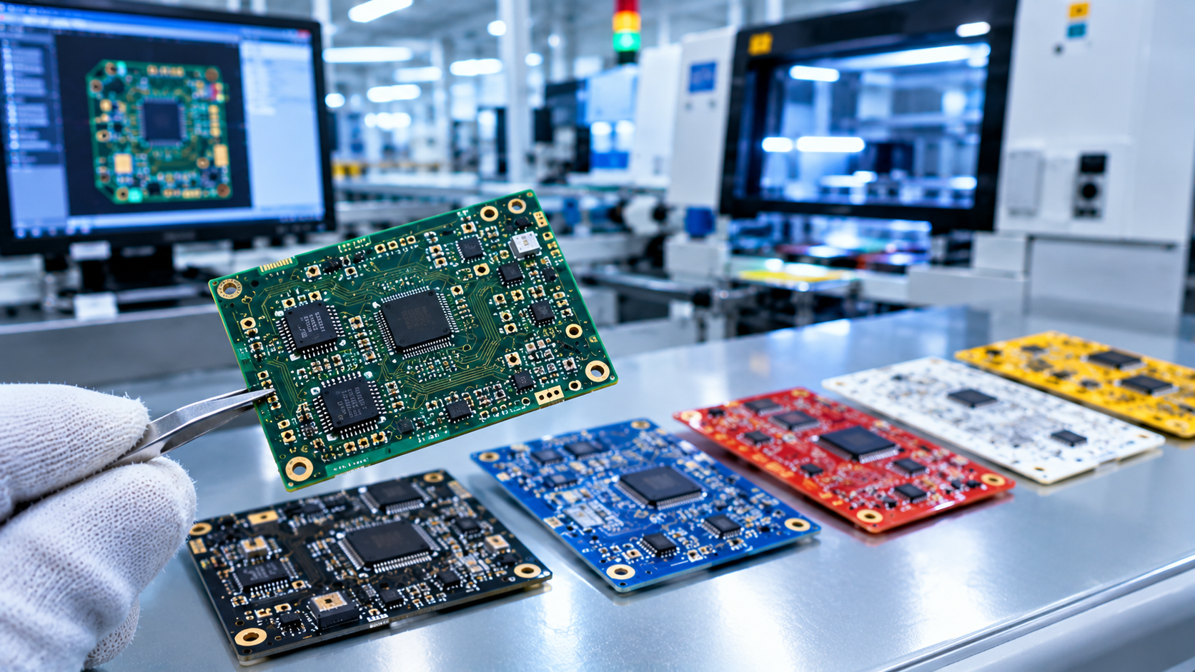
PCB color is determined by the solder mask, and it is more than an aesthetic choice. Color affects AOI inspection, optical alignment, manufacturing cost, lead time, and reliability. This article explains the characteristics of green, white, black, blue, red, and yellow solder masks—and how to choose the right one for your application.

2026.10.10

SMT Incoming Quality Control: The Key to Reliable Electronics Production

Incoming inspection is the first step in SMT assembly quality control and is critical to final product quality. Strict inspection of raw materials—components, PCBs, solder paste, and adhesives—prevents defective parts from entering the production line, avoiding rework, returns, and reputational damage.
2026.10.09

Common Power PCB Layout Mistakes and How to Avoid Them

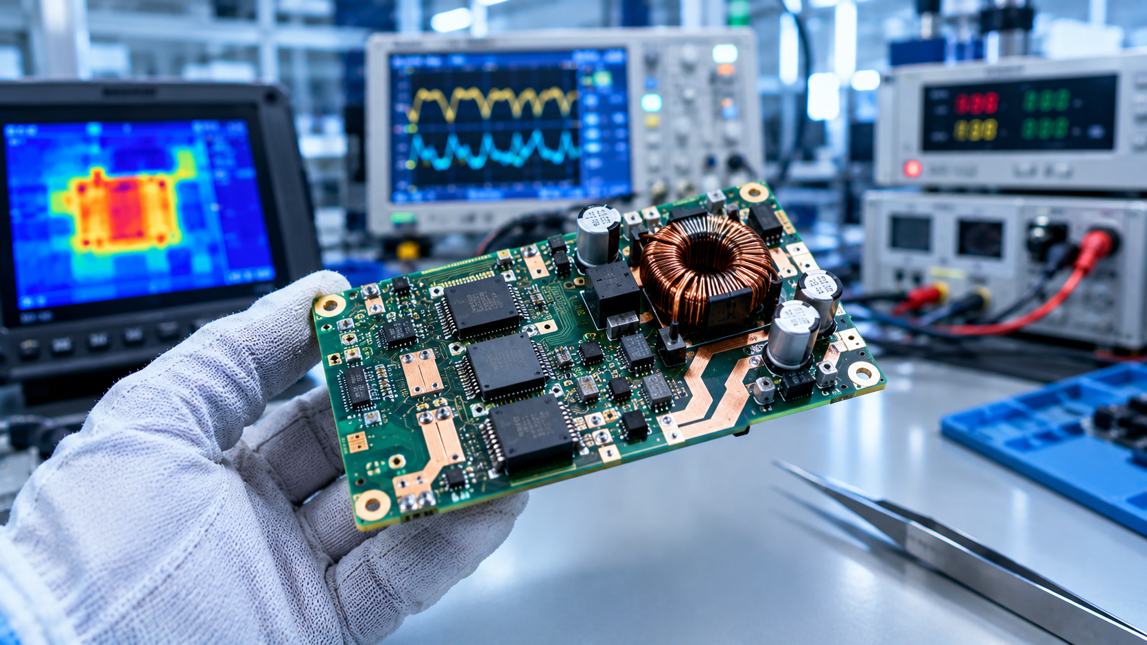
Power supply performance depends heavily on physical PCB layout. Poor layout can cause thermal issues, excessive ripple, EMI problems, and unstable grounding—even in a well-designed circuit. This article covers the most common power PCB layout mistakes in DC/DC and AC/DC designs, their root causes, and practical optimization techniques.
2026.10.09

PCB Via Design Rules: From Through-Holes to Microvias

Vias are essential to PCB layout, connecting traces across layers and delivering power throughout the board. This article covers traditional through-hole vias, blind and buried vias, microvias, annular ring requirements, aspect ratios, and how to manage via rules effectively in modern PCB design.
2026.10.08

PCB Special Processes: The Hidden Skeleton Behind Modern Electronics

From signal transmission to high-density integration, PCB special processes are the core technologies supporting the modern electronics industry. This article covers impedance control, advanced stack-ups, HDI, heavy copper, ENEPIG, 3D-structured PCBs, and industry-specific process selection.
2026.09.23

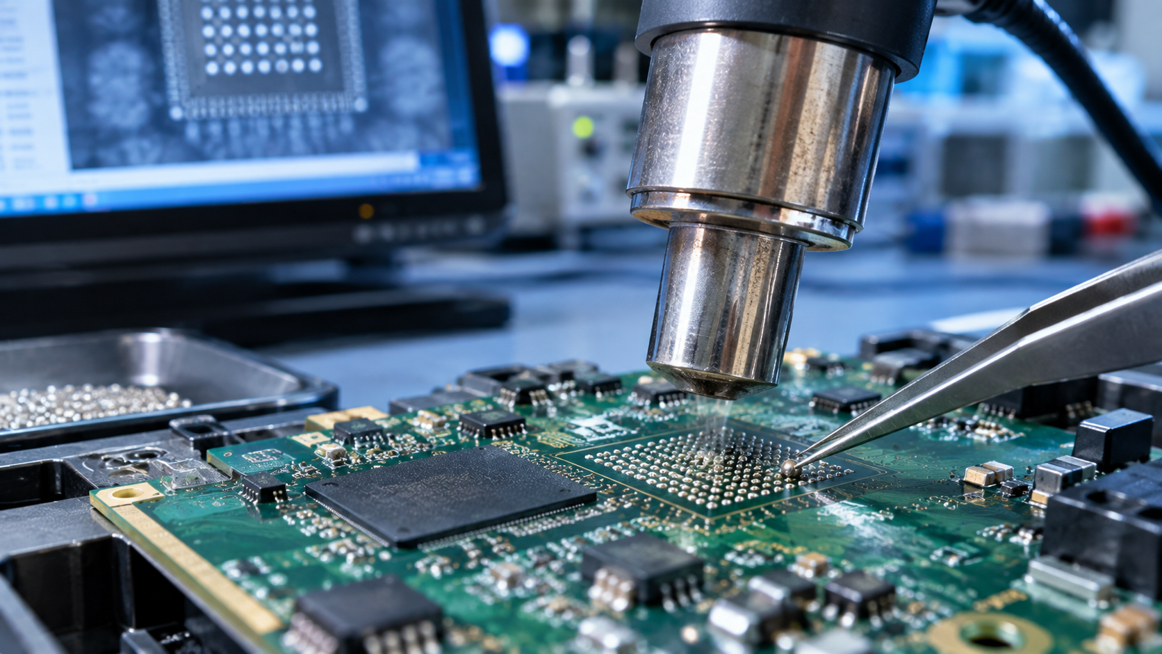
BGA Pad Lifting Failure: 6-Step Repair Guide & Dry Film Application

This article covers the causes of BGA pad lifting and solder bridging, a 6-step repair method, stencil design optimization, reflow profile adjustment, and dry film applications in rework.
2026.09.23

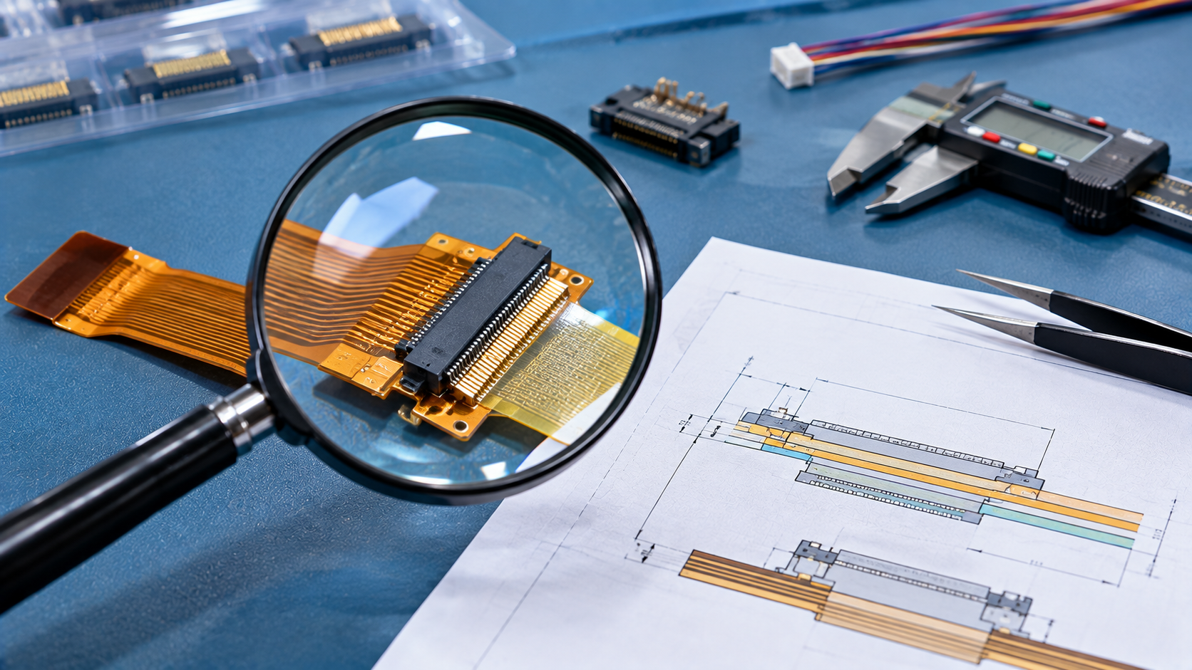
Flexible Circuit Termination Techniques – ZIF, Flying Leads & Crimp Connectors – AnyPCBA

A technical guide to flexible circuit termination techniques. Covers ZIF connectors, unsupported flying leads, crimp connectors, and stiffener design best practices for reliable FPC connections.
2026.09.22

Switching Power Supply & LDO PCB Design Guide – Layout, Grounding & Thermal Tips – AnyPCBA

A practical guide to switching power supply and LDO PCB design. Covers power loop layout, grounding strategy, SENSE/GATE routing, copper pour thermal relief, and thermal via design for reliable power modules.
2026.09.21

Why HDI PCBs Fail in Real Applications – Beyond Microvia Cracking – AnyPCBA

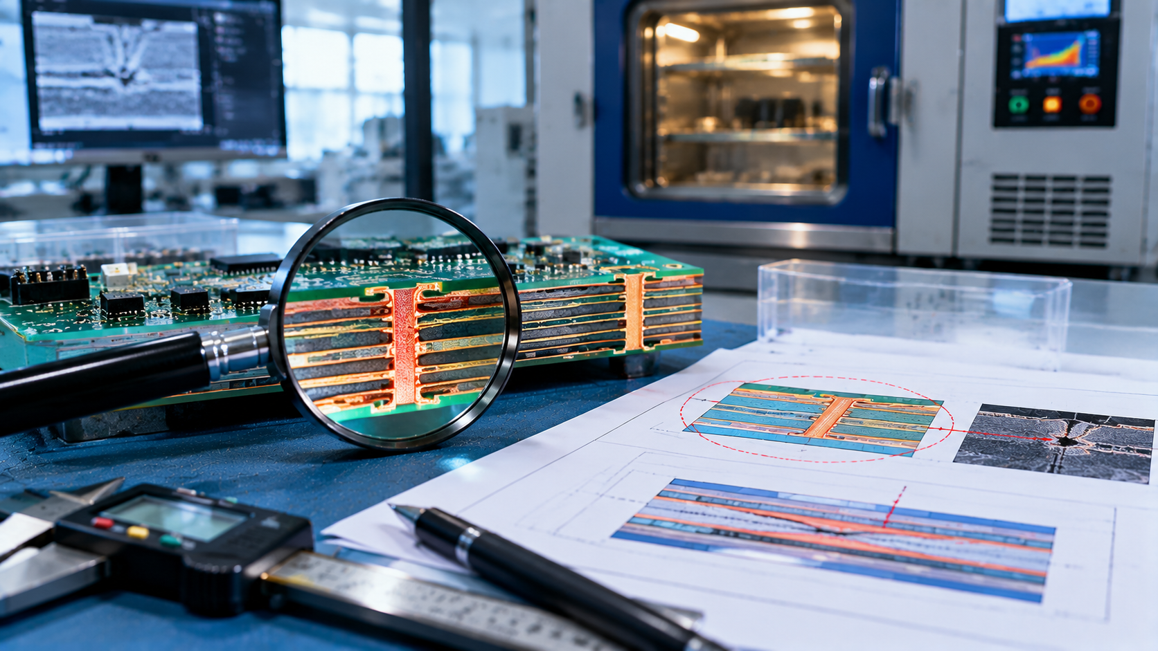
A technical guide to HDI PCB failure mechanisms beyond microvia cracking. Covers resin starvation, copper foil delamination, dielectric crush, CAF growth, and long-term reliability design strategies.
2026.09.20

Multilayer PCB Design Guide – EDA Tools & Best Practices – AnyPCBA

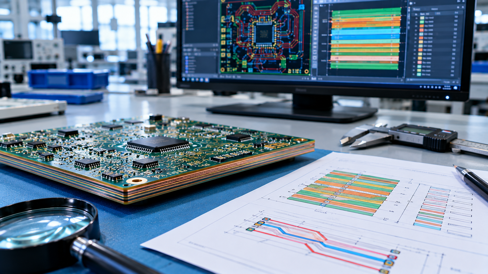
A practical guide to multilayer PCB design. Compare mainstream EDA tools (Altium, Cadence Allegro, Mentor, KiCad), and learn stackup planning, differential routing, via selection, and power/ground strategies.
2026.09.18

PCB Thermal Management Guide – Heat Dissipation Techniques – AnyPCBA

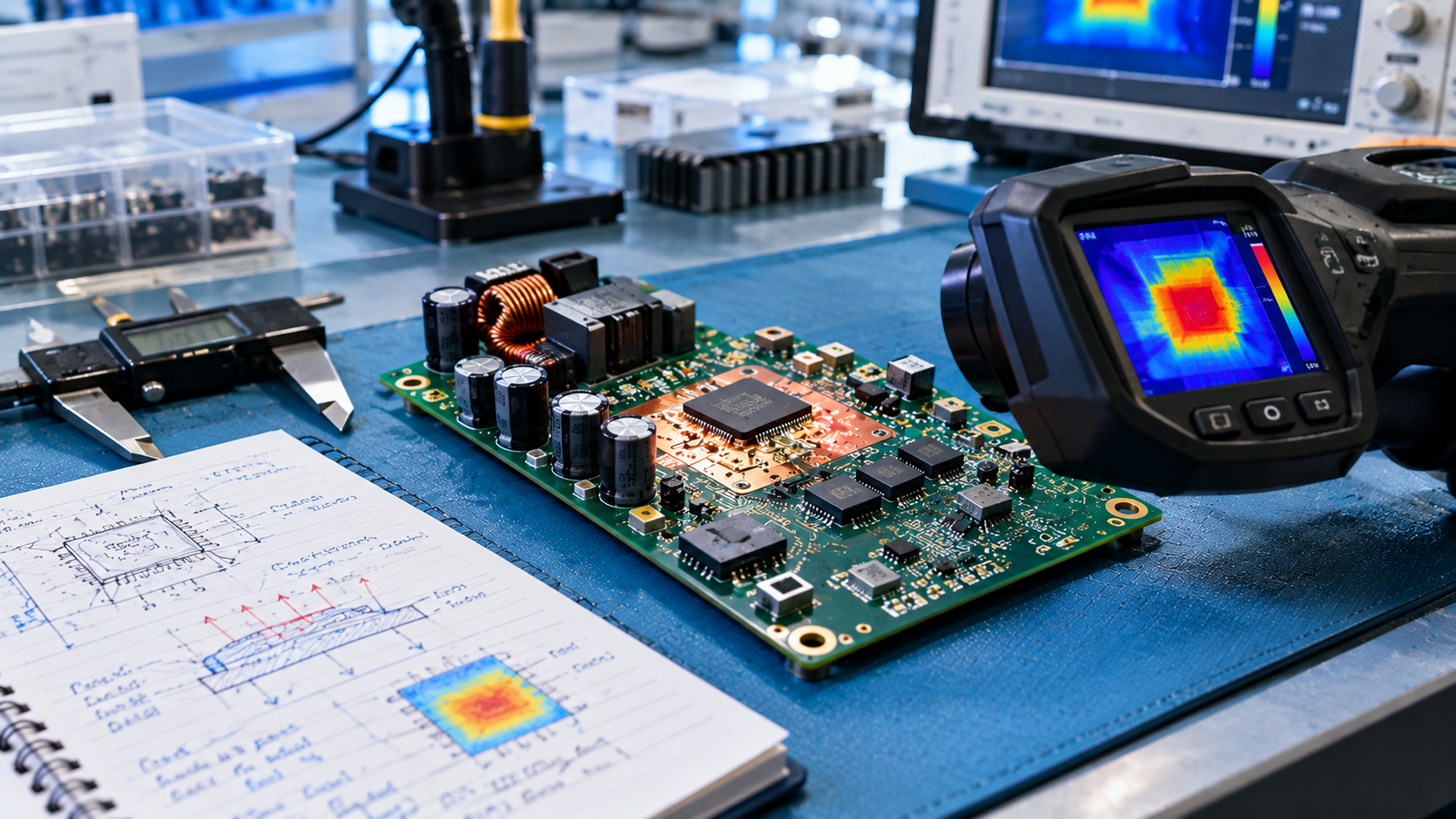
A practical guide to PCB thermal management. Learn heat conduction paths, copper pour strategies, thermal via design, and layout techniques to reduce component temperature and improve reliability.
2026.09.18